MUBW10-06A7 IXYS, MUBW10-06A7 Datasheet - Page 2
MUBW10-06A7
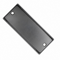
Manufacturer Part Number
MUBW10-06A7
Description
CONVERTER/BRAKE/INVERTER 1.9VCE
Manufacturer
IXYS
Datasheet
1.MUBW10-06A7.pdf
(8 pages)
Specifications of MUBW10-06A7
Igbt Type
NPT
Configuration
Three Phase Inverter with Brake
Voltage - Collector Emitter Breakdown (max)
600V
Vce(on) (max) @ Vge, Ic
2.3V @ 15V, 10A
Current - Collector (ic) (max)
20A
Current - Collector Cutoff (max)
600µA
Input Capacitance (cies) @ Vce
0.6nF @ 25V
Power - Max
85W
Input
Three Phase Bridge Rectifier
Ntc Thermistor
Yes
Mounting Type
Chassis Mount
Package / Case
E2
Vrrm, Rect 1/3 Ph., (v)
1600
Idavm, Tc = 80°c, Rect 1/3 Ph., (a)
18
Rthjc, Typ, Rect 1/3 Ph., (k/w)
1.47
Vces, Inv 3 - Ph., (v)
600
Ic25, Tc = 25°c, Inv 3 - Ph., (a)
20
Ic80, Tc = 80°c, Inv 3 - Ph., (a)
15
Vce(sat), Typ, Tj = 25°c, Inv 3 - Ph., (v)
1.9
Rthjc, Typ, Inv 3 - Ph., (k/w)
1.5
Vces, Br Chopper, (v)
600
Ic80, Tc = 80°c, Br Chopper, (a)
15
Rthjc, Typ, Br Chopper, (k/w)
1.5
Package Style
E2
Lead Free Status / RoHS Status
Lead free / RoHS Compliant
Other names
MUBW1006A7
Available stocks
Company
Part Number
Manufacturer
Quantity
Price
Company:

Part Number:
MUBW10-06A7
Manufacturer:
IXYS
Quantity:
1 000
Part Number:
MUBW10-06A7
Quantity:
60


Symbol
V
V
V
I
I
RBSOA
t
(SCSOA)
P
Symbol
V
V
I
I
t
t
t
t
E
E
C
Q
R
Symbol
I
I
Symbol
V
I
t
R
© 2002 IXYS All rights reserved
Output Inverter T1 - T6
C25
C80
CES
GES
Output Inverter D1 - D6
F25
F80
RM
SC
d(on)
r
d(off)
f
rr
GEM
tot
CE(sat)
GE(th)
on
off
F
CES
GES
ies
thJC
thJC
Gon
Conditions
T
Continuous
Transient
T
T
V
Clamped inductive load; L = 100 µH
V
non-repetitive
T
Conditions
I
I
V
V
V
V
(per IGBT)
Conditions
T
T
Conditions
I
I
V
(per diode)
C
C
F
F
VJ
C
C
C
C
C
GE
CE
CE
CE
CE
CE
R
= 10 A; V
= 15 A; di
= 10 A; V
= 0.4 mA; V
= 25°C
= 80°C
= 25°C
= 25°C
= 80°C
Inductive load, T
V
V
= 300 V; V
= 300V; V
= 25°C to 150°C
= V
= V
= 15 V; R
= 0 V; V
= 25 V; V
CE
GE
CES
CES
= 300 V; I
= ± 15 V; R
; V
; V
GE
GE
F
GE
GE
GE
/dt = -400 A/µs; T
GE
GE
GE
= 0 V; T
= 15 V; T
GE
=
G
= 0 V; T
= 15 V; R
= 0 V; f = 1 MHz
= 15 V; I
= 0 V
= 82
= V
C
G
20 V
= 10 A
VJ
= 82
CE
T
T
T
= 125°C
VJ
VJ
VJ
; T
VJ
VJ
VJ
= 25°C
= 125°C
C
= 25°C
= 125°C
= 25°C
= 125°C
VJ
G
= 10 A
= 82 ; T
= 125°C
VJ
(T
= 125°C
VJ
= 25 C, unless otherwise specified)
VJ
= 125°C
min.
min.
2 - 8
4.5
Characteristic Values
Characteristic Values
I
V
CM
CEK
Maximum Ratings
Maximum Ratings
=
230
600
typ.
typ.
1.9
2.1
0.4
0.4
0.3
1.7
1.2
13
35
35
30
39
90
V
600
CES
20
30
20
15
20
10
85
30
20
max.
max.
200
2.3
6.5
0.6 mA
1.5 K/W
2.0
2.1 K/W
mA
µs
mJ
mJ
W
nA
nC
pF
ns
ns
ns
ns
ns
V
V
V
A
A
A
A
A
V
V
V
V
V
A
Equivalent Circuits for Simulation
Conduction
D11 - D16
Rectifier Diode (typ. at T
T1 - T6 / D1 - D6
IGBT (typ. at V
Free Wheeling Diode (typ. at T
T7 / D7
IGBT (typ. at V
Free Wheeling Diode (typ. at T
Thermal Response
D11 - D16
Rectifier Diode (typ.)
T1 - T6 / D1 - D6
IGBT (typ.)
Free Wheeling Diode (typ.)
T7 / D7
IGBT (typ.)
Free Wheeling Diode (typ.)
C
C
C
C
C
C
C
C
C
C
th1
th2
th1
th2
th1
th2
th1
th2
th1
th2
V
V
= 0.093 J/K; R
= 0.778 J/K; R
= 0.065 J/K; R
= 0.636 J/K; R
= 0.065 J/K; R
= 0.636 J/K; R
= 0.071 J/K; R
= 0.726 J/K; R
= 0.043 J/K; R
V
V
V
= 0.54 J/K; R
0
0
MUBW 10-06 A7
0
0
0
= 0.89 V; R
= 0.89 V; R
= 1.09 V; R
= 1.07 V; R
= 1.11V; R
GE
GE
= 15 V; T
= 15 V; T
th2
0
0
0
th1
th2
th1
th2
th1
th2
th1
th2
th1
0
0
J
= 122 m
= 122 m
= 19 m
= 12 m
= 23 m
= 0.462 K/W
= 125°C)
= 1.212 K/W
= 0.258 K/W
= 1.766 K/W
= 0.344 K/W
= 1.766 K/W
= 0.344 K/W
= 1.211 K/W
= 0.293 K/W
= 2.738 K/W
J
J
= 125°C)
= 125°C)
J
J
= 125°C)
= 125°C)
B4
Related parts for MUBW10-06A7
Image
Part Number
Description
Manufacturer
Datasheet
Request
R

Part Number:
Description:
MODULE IGBT CBI E1
Manufacturer:
IXYS
Datasheet:
Part Number:
Description:
CONVERTER/BRAKE/INVERTER 2.3VCE
Manufacturer:
IXYS
Datasheet:
Part Number:
Description:
MODULE IGBT CBI E1
Manufacturer:
IXYS
Datasheet:

Part Number:
Description:
1600V converter - brake - inverter module
Manufacturer:
IXYS Corporation
Part Number:
Description:
Power Misc, Converter-Brake-Inverter Module
Manufacturer:
IXYS Corporation
Part Number:
Description:
Converter - Brake - Inverter Module
Manufacturer:
IXYS Corporation
Part Number:
Description:
Converter - Brake - Inverter Module
Manufacturer:
IXYS Corporation
Part Number:
Description:
Converter-Brake-Inverter Module
Manufacturer:
IXYS Corporation
Part Number:
Description:
Converter - Brake - Inverter Module (CBI3)
Manufacturer:
IXYS Corporation
Part Number:
Description:
HiPerFET Power MOSFETs
Manufacturer:
IXYS Corporation
Datasheet:
Part Number:
Description:
J-K-Type Flip-Flop
Manufacturer:
IXYS Corporation
Datasheet: