IXFN230N10 IXYS, IXFN230N10 Datasheet

MOSFET N-CH 100V 230A SOT-227B

IXFN230N10

Manufacturer Part Number
IXFN230N10
Description
MOSFET N-CH 100V 230A SOT-227B
Manufacturer
IXYS
Series
HiPerFET™r
Datasheet

Specifications of IXFN230N10

Fet Type
MOSFET N-Channel, Metal Oxide
Fet Feature
Standard
Rds On (max) @ Id, Vgs
6 mOhm @ 500mA, 10V
Drain To Source Voltage (vdss)
100V
Current - Continuous Drain (id) @ 25° C
230A
Vgs(th) (max) @ Id
4V @ 8mA
Gate Charge (qg) @ Vgs
570nC @ 10V
Input Capacitance (ciss) @ Vds
19000pF @ 25V
Power - Max
700W
Mounting Type
Chassis Mount
Package / Case
SOT-227, miniBLOC
Configuration
Single Dual Source
Transistor Polarity
N-Channel
Resistance Drain-source Rds (on)
0.0065 Ohms
Drain-source Breakdown Voltage
100 V
Gate-source Breakdown Voltage
+/- 20 V
Continuous Drain Current
230 A
Power Dissipation
700 W
Maximum Operating Temperature
+ 150 C
Mounting Style
SMD/SMT
Minimum Operating Temperature
- 55 C
Vdss, Max, (v)
100
Id(cont), Tc=25°c, (a)
230
Rds(on), Max, Tj=25°c, (?)
0.006
Ciss, Typ, (pf)
19000
Qg, Typ, (nc)
570
Trr, Typ, (ns)
-
Trr, Max, (ns)
250
Pd, (w)
700
Rthjc, Max, (ºc/w)
0.18
Package Style
SOT-227B
Lead Free Status / RoHS Status
Lead free / RoHS Compliant

Available stocks

Company
Part Number
Manufacturer
Quantity
Price
Part Number:
IXFN230N10
Manufacturer:
IXYS
Quantity:
200
Part Number:
IXFN230N10
Quantity:
130
Power MOSFET
Single Die MOSFET
N-Channel Enhancement Mode
Avalanche Rated, High dv/dt, Low t
Symbol
V
V
V
V
I
I
I
I
E
dV/dt
P
T
T
T
V
M
Weight
Symbol
(T
BV
V
I
I
R
D25
L(RMS)
DM
A
GSS
DSS
© 2008 IXYS Corporation, All rights reserved
J
JM
stg
DSS
DGR
GSS
GSM
AS
d
ISOL
GS(th)
DS(on)
d
J
DSS
= 25°C, unless otherwise specified)
Test Conditions
T
T
Continuous
Transient
T
External lead current limit
T
T
T
I
T
50/60 Hz, RMS
I
Mounting torque
Terminal connection torque
V
V
V
V
V
V
Test Conditions
S
ISOL
J
J
C
C
C
C
C
GS
DS
GS
DS
GS
GS
= 25°C to 150°C
= 25°C to 150°C, R
= 25°C, Chip capability
= 25°C, pulse width limited by T
= 25°C
= 25°C
≤ I
= 25°C
≤ 1mA
= 0V, I
= V
= ±20V, V
= V
= 0V
= 10V, I
DM
, V
GS
DSS
, I
DD
D
D
D
= 3mA
≤ V
= 8mA
= 0.5 • I
DS
DSS
= 0V
t = 1min
t = 1s
, T
D25
J
GS
≤ 150°C
, Note 1
= 1MΩ
T
J
= 125°C
rr
JM
IXFN230N10
Min.
100
Characteristic Values
2.0
-55 ... +150
-55 ... +150
Maximum Ratings
1.3/11.5
1.5/13
Typ.
2500
3000
100
100
±20
±30
230
200
920
100
700
150
10
30
4
±200
Max.
100
4.0
6.0
Nm/lb.in.
Nm/lb.in.
2
V/ns
mA
V~
V~
μA
nA
°C
°C
°C
W
V
V
V
V
A
A
A
A
g
V
V
J
V
I
R
t
Features
Advantages
Applications
G = Gate
S = Source
Either Source terminal at miniBLOC can be used
as Main or Kelvin Source
miniBLOC, SOT-227 B
D25
rr
International standard package
miniBLOC, with Aluminium nitride
isolation
Low R
Rugged polysilicon gate cell structure
Avalanche rated
Guaranteed FBSOA
Low package inductance
Fast intrinsic Rectifier
Easy to mount
Space savings
High power density
DC-DC converters
Battery chargers
Switched-mode and resonant-mode
power supplies
DC choppers
Temperature and lighting controls
DS(on)
DSS
E153432
DS (on)
= 100V
= 230A
≤ ≤ ≤ ≤ ≤ 6.0mΩ Ω Ω Ω Ω
≤ ≤ ≤ ≤ ≤ 250ns
HDMOS
G
D = Drain
S
TM
process
DS98548F(12/08)
D
S

Related parts for IXFN230N10

IXFN230N10 Summary of contents

Page 1

... D = ±20V GSS DSS DS DSS 10V 0.5 • I DS(on D25 © 2008 IXYS Corporation, All rights reserved IXFN230N10 rr Maximum Ratings 100 = 1MΩ 100 GS ±20 ±30 230 200 920 JM 100 4 ≤ 150°C 10 700 -55 ... +150 150 -55 ... +150 2500 3000 1.5/13 1.3/11.5 30 Characteristic Values Min ...

Page 2

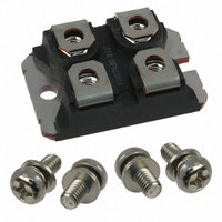
... I = 0.5 • DSS D D25 290 0.05 Characteristic Values Min. Typ 50V 1.2 R 9.0 4,931,844 5,049,961 5,237,481 6,162,665 5,017,508 5,063,307 5,381,025 6,259,123 B1 5,034,796 5,187,117 5,486,715 6,306,728 B1 IXFN230N10 miniBLOC, SOT-227 B Max screws (4x) supplied nC Dim. Millimeter Min. Max 31.50 31. 7.80 C 4.09 0.18 °C ...

Page 3

... Value D 220 200 180 160 T = 125ºC J 140 120 100 T = 25ºC J 200 250 300 350 IXFN230N10 Fig. 2. Extended Output Characteristics @ 25º 10V 0.0 0.5 1.0 1.5 2.0 2.5 3 Volts DS Fig Normalized to I DS(on) vs ...

Page 4

... T = 25º 0.8 0.9 1.0 1.1 1.000 C iss 0.100 C oss 0.010 C rss 0.001 0.0001 IXFN230N10 Fig. 8. Transconductance 100 120 I - Amperes D Fig. 10. Gate Charge V = 50V 100A 10mA 100 150 200 250 300 350 400 Q - NanoCoulombs G Fig. 12. Maximum Transient Thermal Impedance ...

Page 5

... IXYS Corporation, All rights reserved Fig. 14. Forward-Bias Safe Operating Area 1,000 R Limit DS(on) 100µs 1ms 100 10ms 100ms 150º 75ºC C Single Pulse 1 100 1 IXFN230N10 @ T = 75ºC C 25µs 100µs 1ms 10ms 100ms DC 10 100 V - Volts DS IXYS REF: F_230N10(9Y-N17)12-02-08-D ...

Related keywords