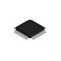
ST16C450CQ48-F Exar Corporation, ST16C450CQ48-F Datasheet - Page 15

ST16C450CQ48-F
Manufacturer Part Number
ST16C450CQ48-F
Description
IC UART SINGLE 48TQFP
Manufacturer
Exar Corporation
Type
UARTsr
Datasheet
1.ST16C450CJ44TR-F.pdf
(28 pages)
Specifications of ST16C450CQ48-F
Package / Case
48-TQFP
Features
*
Number Of Channels
1, UART
Fifo's
1 Byte
Voltage - Supply
2.97 V ~ 5.5 V
With False Start Bit Detection
Yes
With Modem Control
Yes
With Cmos
Yes
Mounting Type
Surface Mount
Data Rate
1.5 Mbps
Supply Current
3 mA
Maximum Operating Temperature
0 C
Minimum Operating Temperature
+ 70 C
Mounting Style
SMD/SMT
Operating Supply Voltage
7 V
Lead Free Status / RoHS Status
Lead free / RoHS Compliant
Lead Free Status / RoHS Status
Lead free / RoHS Compliant, Lead free / RoHS Compliant
Available stocks
Company
Part Number
Manufacturer
Quantity
Price
Company:
Part Number:
ST16C450CQ48-F
Manufacturer:
EXAR
Quantity:
1 400
Company:
Part Number:
ST16C450CQ48-F
Manufacturer:
Exar Corporation
Quantity:
10 000
LCR BIT-5 = logic 0, parity is not forced (normal default
condition)
LCR BIT-5 = logic 1 and LCR BIT-4 = logic 0, parity bit
is forced to a logical 1 for the transmit and receive
data.
LCR BIT-5 = logic 1 and LCR BIT-4 = logic 1, parity bit
is forced to a logical 0 for the transmit and receive
data.
LCR BIT-6:
When enabled the Break control bit causes a break
condition to be transmitted (the TX output is forced to
a logic 0 state). This condition exists until disabled by
setting LCR bit-6 to a logic 0.
Logic 0 = No TX break condition. (normal default
condition)
Logic 1 = Forces the transmitter output (TX) to a logic
0 for alerting the remote receiver to a line break
condition.
LCR BIT-7:
The internal baud rate counter latch and Enhance
Feature mode enable.
Logic 0 = Divisor latch disabled. (normal default
condition)
Logic 1 = Divisor latch and enhanced feature register
enabled.
Modem Control Register (MCR)
This register controls the interface with the modem or a
peripheral device.
MCR BIT-0:
Logic 0 = Force -DTR output to a logic 1. (normal
default condition)
Logic 1 = Force -DTR output to a logic 0.
Bit-5
LCR
Rev. 4.20
X
0
0
1
1
Bit-4
LCR
X
0
1
0
1
Bit-3
LCR
0
1
1
1
1
Parity selection
No parity
Odd parity
Even parity
Force parity”1”
Forced parity “0”
15
MCR BIT-1:
Logic 0 = Force -RTS output to a logic 1. (normal default
condition)
Logic 1 = Force -RTS output to a logic 0.
MCR BIT-2:
Logic 0 = Set -OP1 output to a logic 1. (normal default
condition)
Logic 1 = Set -OP1 output to a logic 0.
MCR BIT-3:
Logic 0 = Set -OP2 output to a logic 1. (normal default
condition)
Logic 1 = Set -OP2 output to a logic 0.
MCR BIT-4:
Logic 0 = Disable loop-back mode. (normal default
condition)
Logic 1 = Enable local loop-back mode (diagnostics).
MCR BIT 5-7: Not used and set to “0”.
Line Status Register (LSR)
This register provides the status of data transfers
between. the ST16C450 and the CPU.
LSR BIT-0:
Logic 0 = No data in receive holding register. (normal
default condition)
Logic 1 = Data has been received and is saved in the
receive holding register.
LSR BIT-1:
Logic 0 = No overrun error. (normal default condition)
Logic 1 = Overrun error. A data overrun error occurred
in the receive shift register. This happens when addi-
tional data arrives while the RHR is full. In this case the
previous data in the shift register is overwritten. Note
that under this condition the data byte in the receive
shift register is not transfer into the RHR, therefore the
data in the RHR is not corrupted by the error.
LSR BIT-2:
Logic 0 = No parity error (normal default condition)
Logic 1 = Parity error. The receive character does not
have correct parity information and is suspect.
ST16C450


