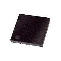
XR18W753IL48-F Exar Corporation, XR18W753IL48-F Datasheet - Page 4

XR18W753IL48-F
Manufacturer Part Number
XR18W753IL48-F
Description
IC RF TXRX 868-956MHZ 48QFN
Manufacturer
Exar Corporation
Type
RF Receiversr
Series
-r
Datasheet
1.XR18W753IL48-F.pdf
(27 pages)
Specifications of XR18W753IL48-F
Package / Case
48-VFQFN Exposed Pad
Frequency
868MHz ~ 954MHz
Data Rate - Maximum
250kbps
Modulation Or Protocol
DSSS
Applications
ISM
Power - Output
0dBm
Sensitivity
-94dBm
Voltage - Supply
2.2 V ~ 3.6 V
Current - Receiving
19mA
Current - Transmitting
22mA
Data Interface
PCB, Surface Mount
Antenna Connector
PCB, Surface Mount
Operating Temperature
-40°C ~ 85°C
Operating Frequency
100 KHz, 400 KHz
Operating Supply Voltage
2.2 V to 3.6 V
Maximum Operating Temperature
+ 85 C
Minimum Operating Temperature
- 40 C
Mounting Style
SMD/SMT
Noise Figure
12 dB
Supply Current
0.5 mA, 1.7 mA, 19 mA, 22 mA
Data Rate
250Kbps
Rf Ic Case Style
QFN
No. Of Pins
48
Supply Voltage Range
2.97V To 3.63V
Operating Temperature Range
-40°C To +85°C
Memory Size
-
Lead Free Status / RoHS Status
Lead free / RoHS Compliant
Lead Free Status / RoHS Status
Lead free / RoHS Compliant, Lead free / RoHS Compliant
Available stocks
Company
Part Number
Manufacturer
Quantity
Price
Part Number:
XR18W753IL48-F
Manufacturer:
EXAR/艾科嘉
Quantity:
20 000
XR18W753
SINGLE CHIP 868MHZ TO 956MHZ RF TRANSCEIVER
PIN DESCRIPTIONS
VDD_VCO
AVDD19
AVDD19
AVDD19
AVDD19
RFCM1
RFCM2
TEST0
TEST1
RFIN+
DGND
AGND
AGND
AGND
AGND
AGND
AGND
RFIN-
AVDD
N
ATO+
ATO-
IRQ#
ATI+
SCL
SDA
R1+
ATI-
R1-
A0
A1
AME
P
10
11
12
13
14
15
16
17
18
19
20
21
22
23
24
25
26
27
28
29
30
1
2
3
4
5
6
7
8
9
IN
Analog I/O
Analog I/O
Analog I/O
DigitaI OD
Digital OD
Analog O
Analog O
Analog O
Analog O
Analog O
Digital O
Analog I
Analog I
Ground
Power I
Ground
Power I
Power I
Ground
Power I
Ground
Power I
Ground
Ground
Ground
Digital I
Digital I
Digital I
Digital I
T
YPE
Analog ground for IF part of RX and BB part of TX
Analog VDD (1.9V ± 0.1V) for IF part of RX and BB part of TX.
Analog ground for RX frontend and PA
Analog VDD (1.9V ± 0.1V) for LNA and PA.
Common Mode voltage output for matching network.
Voltage output TX: 1.9V RX: ≈ 170mV
Differential RF signals
Common Mode voltage output for matching network.
Voltage output TX: 1.9V RX: ≈ 170mV
Analog VDD (1.9V ± 0.1V) for LNA and PA.
Analog ground for RX frontend and PA
Analog VDD (1.9V ± 0.1V) for LNA and PA.
Analog ground for IF part of RX and BB part of TX.
External resistor to fix PA power. 470 ohm resistor connected between
R1- and R1+ is recommended.
Analog VDD (1.9V ± 0.1V) for synthesizer.
Analog ground for synthesizer.
VDD of VCO. VDD = 1.9V ± 0.1V (for decoupling).
Analog ground for VCO.
Analog Test Input
Analog Test Input
Analog Test Output
Analog Test Output
Digital ground
Factory Test Mode. For normal operation, this pin should be connected
to GND.
Open-drain I2C serial clock
Open-drain I2C serial data
I2C Address bit-0
I2C Address bit-1
Interrupt output (active low, open-drain).
Factory Test Mode. For normal operation, this pin should be connected
to GND.
4
D
ESCRIPTION
REV. 1.0.0


