TBU-PK085-100-WH Bourns Inc., TBU-PK085-100-WH Datasheet
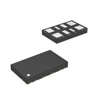
SURGE SUPP TBU DL 100MA 850VIMP

TBU-PK085-100-WH

Manufacturer Part Number
TBU-PK085-100-WH
Description
SURGE SUPP TBU DL 100MA 850VIMP
Manufacturer
Bourns Inc.
Series
TBU-PKr

Specifications of TBU-PK085-100-WH

Package / Case
SMD 6.50mm x 4.00mm
Voltage - Working
425V
Voltage - Clamping
850V
Technology
Mixed Technology
Number Of Circuits
2
Applications
SLIC
Voltage Rating
850 V
Current Rating
150 mA
Termination Style
SMD/SMT
Diode Type
Bidirectional TVS
Operating Voltage
850V
Diode Case Style
DFN
No. Of Pins
8
Response Time
1µs
Rohs Compliant
Yes
Lead Free Status / RoHS Status
Lead free / RoHS Compliant
Power (watts)
-
Lead Free Status / Rohs Status
Lead free / RoHS Compliant
Other names
TBU-PK085-100-WHTR
The TBU-PK Series of Bourns
protection components, constructed using MOSFET semiconductor technology, and designed to
protect against faults caused by short circuits, AC power cross, induction and lightning surges.
In addition to overcurrent protection, an added feature is the voltage monitoring on the two lines. If the
voltage on the line drops below V ss then the voltage will trigger the device to switch to the blocking
state.
The TBU
detection circuit triggering to provide an effective barrier behind which sensitive electronics will not be
exposed to large voltages or currents during surge events. The TBU
mount DFN package and meets industry standard requirements such as RoHS and Pb Free solder
refl ow profi les.
*RoHS Directive 2002/95/EC Jan 27, 2003 including Annex.
Specifi cations are subject to change without notice.
Customers should verify actual device performance in their specifi c applications.
UL
Symbol
I
R
R
t
I
I
V
V
V
R
R
trigger
Q
ss
Symbol
V
V
T
T
T
ESD
block
General Information
Absolute Maximum Ratings (@ T
Electrical Characteristics (@ T
Agency Approval
reset
to
ss
device
match
th(j-l)
th(j-l)
op
stg
jmax
imp
rms
®
high speed protector placed in the system circuit will monitor the current with the MOSFET
File Number: E315805
Parameter
Current required for the device to go from operating state to protected state
Series resistance of the TBU
Package resistance matching of the TBU
Time taken for the device to go into current limiting
Current through the triggered TBU
Operating current with V
Voltage below which the triggered TBU
operating state
Voltage threshold offset with 60 Hz applied voltage, with V
Operating voltage range relative to V dd
Junction to package pads - FR4 using minimum recommended pad layout
Junction to package pads - FR4 using heat sink on board (6 cm
Parameter
Peak impulse voltage withstand with duration less than 10 ms
Continuous A.C. RMS voltage
Operating temperature range
Storage temperature range
Maximum junction temperature
HBM ESD protection per IEC 61000-4-2 on line pads
Description
®
TBU
®
A
ss
products are low capacitance dual bidirectional high speed
= 25 °C Unless Otherwise Noted)
A
= -50 V
= 25 °C Unless Otherwise Noted)
®
device
®
device with 50 Vdc circuit voltage
TBU-PK Series - TBU
Features
Solutions available for GR-1089-CORE, ITU-T and a combination of both.
Industry Standards (in Conjunction with OVP Device)
®
Superior circuit protection
Overcurrent & overvoltage protection
Blocks surges up to rated limits
High speed performance
Small SMT package
RoHS compliant*
Agency recognition:
device will transition to normal
®
device #1 - TBU
®
device is provided in a surface
ss
®
device #2
-50 V (V
2
) (0.5 in.
ss
TBU-PK050-100-WH
TBU-PK060-100-WH
TBU-PK075-100-WH
TBU-PK085-100-WH
TBU-PK050-100-WH
TBU-PK060-100-WH
TBU-PK075-100-WH
TBU-PK085-100-WH
- V
®
2
Part Number
)
lineSLIC
High Speed Protectors
)
Applications
SLIC protection
Cable & DSL
MDU/MTU modems
ONT
Voice/DSL line cards
Min.
-180
0.25
100
-1.0
65
12
Line 1 SLIC
Line 2 SLIC
-55 to +125
-65 to +150
±0.5
Typ.
0.70
Value
150
100
+125
80
15
65
40
500
600
750
850
300
350
400
425
±2
TBU
Max.
±1.6
1.50
200
-20
®
0.2
90
22
1
Device
V dd
V ss
Unit
°C
°C
°C
kV
Line 1
Line 2
V
V
°C/W
°C/W
Unit
mA
mA
µA
µs
Ω
Ω
V
V
V

Related parts for TBU-PK085-100-WH

TBU-PK085-100-WH Summary of contents

Page 1

... Industry Standards (in Conjunction with OVP Device) Solutions available for GR-1089-CORE, ITU-T and a combination of both. TBU-PK050-100-WH TBU-PK060-100-WH TBU-PK075-100-WH TBU-PK085-100-WH TBU-PK050-100-WH TBU-PK060-100-WH TBU-PK075-100-WH TBU-PK085-100-WH ® device ® device #1 - TBU ® device #2 ® device with 50 Vdc circuit voltage ® device will transition to normal ...

Page 2

... TBU-PK Series - TBU Functional Block Diagram Reference Application The TBU-PK Series are high-speed protectors used in voice/ VolP SLIC applications. The maximum voltage rating of the TBU ® device should never be exceeded. Where necessary, an OVP device should be employed to limit the maximum voltage. ...

Page 3

... V rms, 200 Ω 2s 5000 V, 500 A 2/10 µs 120V RMS 900 s 1500 V, 40 Ω 10/700 µs 6000 V, 40 Ω 10/700 µs* TBU-PK085-100-WH 230 V rms 10 Ω -1000 Ω, 900 s 600 V rms 600 Ω, 0.2 s 600 V rms 600 Ω 1500 V rms, 200 Ω 2s* ...

Page 4

... TBU-PK Series - TBU ® Performance Graphs Typical V-I Characteristics (TBU-PK085-100-WH) CURRENT I TRIP (50 mA/div) Tracking Voltage Characteristics V bat range of - -150 V 100 Voltage threshold offset (V) Power Derating Curve 3.0 One Side, No PCB Cu One Side, 0.5 sq. in. PCB Cu 2.5 Two Sides, No PCB Cu Two Sides, 0.5 sq. in. PCB Cu 2 ...

Page 5

... C PIN 1 0.75 (.010) (.030) 1.30 0.70 (.051) (.028) 0.75 0.75 (.030) (.030) 0.40 (.016) 120 ® Power in One Side of TBU Device Total Power in Both Sides of TBU 100 0.2 0.4 0.6 0.8 1.0 1.2 1.4 Added Cu Area (Sq. In.) ® Device 1.6 1.8 ...

Page 6

... Time (tsmin to tsmax) Time maintained above: - Temperature (TL) - Time (tL) Peak/Classifi cation Temperature (Tp) Time within 5 °C of Actual Peak Temp. (tp) Ramp-Down Rate Time 25 °C to Peak Temperature How to Order TBU - PK 085 - 100 - WH ® TBU Product Series PK = Dual Bidirectional Series Impulse Voltage Rating 050 = 500 V 060 = 600 V ...

Page 7

... REV. 01/11 “TBU” registered trademark of Bourns, Inc. in the U.S., Taiwan and European Community. Specifi cations are subject to change without notice. Customers should verify actual device performance in their specifi c applications. High Speed Protectors D t TOP ...

Related keywords