BLF7G20LS-160P,118 NXP Semiconductors, BLF7G20LS-160P,118 Datasheet
BLF7G20LS-160P,118
Specifications of BLF7G20LS-160P,118


Related parts for BLF7G20LS-160P,118


BLF7G20LS-160P,118 Summary of contents
Page 1
... BLF7G20L-160P; BLF7G20LS-160P Power LDMOS transistor Rev. 01 — 22 June 2010 1. Product profile 1.1 General description 160 W LDMOS power transistor for base station applications at frequencies from 1800 MHz to 2000 MHz. Table 1. Typical performance Typical RF performance case Mode of operation f (MHz) CW 1805 to 1880 GSM EDGE 1805 to 1880 1 ...
Page 2
... BLF7G20LS-160P - 4. Limiting values Table 4. In accordance with the Absolute Maximum Rating System (IEC 60134). Symbol stg T j BLF7G20L-160P_7G20LS-160P Objective data sheet BLF7G20L-160P; BLF7G20LS-160P Pinning Description drain1 drain2 gate1 gate2 source drain1 drain2 gate1 gate2 source Ordering information Package Name Description - flanged LDMOST ceramic package; 2 mounting holes; ...
Page 3
... EVM M Mode of operation: CW η D 7.1 Ruggedness in class-AB operation The BLF7G20L-160P and BLF7G20LS-160P are capable of withstanding a load mismatch corresponding to VSWR = through all phases under the following conditions: V BLF7G20L-160P_7G20LS-160P Objective data sheet BLF7G20L-160P; BLF7G20LS-160P Thermal characteristics Parameter thermal resistance from junction to case Characteristics C ...
Page 4
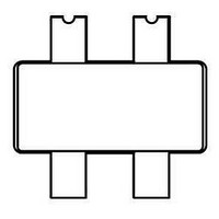
... Note 1. millimeter dimensions are derived from the original inch dimensions. 2. dimension is measured 0.030 inch (0.76 mm) from the body. Outline version IEC SOT1121A Fig 1. Package outline SOT1121A BLF7G20L-160P_7G20LS-160P Objective data sheet BLF7G20L-160P; BLF7G20LS-160P scale D ...
Page 5
... Note 1. millimeter dimensions are derived from the original inch dimensions. 2. dimension is measured 0.030 inch (0.76 mm) from the body. Outline version IEC SOT1121B Fig 2. Package outline SOT1121B BLF7G20L-160P_7G20LS-160P Objective data sheet BLF7G20L-160P; BLF7G20LS-160P scale ...
Page 6
... VSWR W-CDMA 10. Revision history Table 9. Revision history Document ID BLF7G20L-160P_7G20LS-160P v.1 BLF7G20L-160P_7G20LS-160P Objective data sheet BLF7G20L-160P; BLF7G20LS-160P Abbreviations Description Continuous Wave Enhanced Data rates for GSM Evolution ElectroStatic Discharge Interim Standard 95 Laterally Diffused Metal Oxide Semiconductor Laterally Diffused Metal Oxide Semiconductor Transistor ...
Page 7
... BLF7G20L-160P_7G20LS-160P Objective data sheet BLF7G20L-160P; BLF7G20LS-160P [3] Definition This document contains data from the objective specification for product development. This document contains data from the preliminary specification. ...
Page 8
... For sales office addresses, please send an email to: BLF7G20L-160P_7G20LS-160P Objective data sheet BLF7G20L-160P; BLF7G20LS-160P NXP Semiconductors’ specifications such use shall be solely at customer’s own risk, and (c) customer fully indemnifies NXP Semiconductors for any liability, damages or failed product claims resulting from customer design and use of the product for automotive applications beyond NXP Semiconductors’ ...
Page 9
... Trademarks Contact information Contents . . . . . . . . . . . . . . . . . . . . . . . . . . . . . . . 9 BLF7G20L-160P; BLF7G20LS-160P Please be aware that important notices concerning this document and the product(s) described herein, have been included in section ‘Legal information’. © NXP B.V. 2010. For more information, please visit: http://www.nxp.com For sales office addresses, please send an email to: salesaddresses@nxp.com Power LDMOS transistor All rights reserved ...