BLF7G20LS-250P,118 NXP Semiconductors, BLF7G20LS-250P,118 Datasheet
BLF7G20LS-250P,118
Specifications of BLF7G20LS-250P,118


Related parts for BLF7G20LS-250P,118


BLF7G20LS-250P,118 Summary of contents
Page 1
... BLF7G20L-250P; BLF7G20LS-250P Power LDMOS transistor Rev. 3 — 1 March 2011 1. Product profile 1.1 General description 250 W LDMOS power transistor for base station applications at frequencies from 1805 MHz to 1880 MHz. Table 1. Typical RF performance at T Mode of operation 2-carrier W-CDMA [1] Test signal: 3GPP; test model 1;64 DPCH; PAR = 8 0.01% probability on CCDF. ...
Page 2
... NXP Semiconductors 2. Pinning information Table 2. Pin BLF7G20L-250P (SOT539A BLF7G20LS-250P (SOT539B [1] Connected to flange. 3. Ordering information Table 3. Type number BLF7G20L-250P BLF7G20LS-250P 4. Limiting values Table 4. In accordance with the Absolute Maximum Rating System (IEC 60134). Symbol stg T j BLF7G20L-250P_7G20LS-250P Product data sheet BLF7G20L-250P; BLF7G20LS-250P ...
Page 3
... P L(AV D ACPR 7.1 Ruggedness in class-AB operation The BLF7G20L-250P and BLF7G20LS-250P are capable of withstanding a load mismatch corresponding to a VSWR = through all phases under the following conditions: V 1880 MHz. BLF7G20L-250P_7G20LS-250P Product data sheet BLF7G20L-250P; BLF7G20LS-250P Thermal characteristics Parameter thermal resistance from junction to case Characteristics C unless otherwise specified ...
Page 4
... Measured load-pull data half device (MHz) 1750 1805 1845 1880 1930 [1] Z and Z S Fig 1. BLF7G20L-250P_7G20LS-250P Product data sheet BLF7G20L-250P; BLF7G20LS-250P Typical impedance = 950 mA [ () 1.31 j3.53 1.39 j3.75 1.48 j4.10 1.55 j4.19 1.97 j4.48 defined in Figure 1 ...
Page 5
... D (%) 100 ( 1805 MHz. ( 1845 MHz. ( 1880 MHz. Fig 4. Efficiency as a function of average output power; typical values BLF7G20L-250P_7G20LS-250P Product data sheet BLF7G20L-250P; BLF7G20LS-250P 001aal942 (1) (2) (3) ACPR (dBc) 250 350 P (W) L(M) ( 1805 MHz. ( 1845 MHz. ( 1880 MHz. Fig 3. 001aal950 G ...
Page 6
... MHz. ( 1845 MHz. ( 1880 MHz. Fig 6. Power gain as a function of average output power; typical values BLF7G20L-250P_7G20LS-250P Product data sheet BLF7G20L-250P; BLF7G20LS-250P = 1900 mA. Dq 001aal949 (1) (2) (3) 200 300 P (W) L(AV) Fig 7. All information provided in this document is subject to legal disclaimers. Rev. 3 — 1 March 2011 ...
Page 7
... D 17.0 16.5 16 Fig 10. Average power gain and drain efficiency as a function of average output power; typical values BLF7G20L-250P_7G20LS-250P Product data sheet BLF7G20L-250P; BLF7G20LS-250P = 1900 mA; channel spacing = 5 MHz; PAR = 8 0.01 % probability Dq 001aal946 η D (1) (%) (2) (3) 100 120 140 P (W) L(AV) ( 1805 MHz ...
Page 8
... BLF7G20L-250P Input Rev 03 Printed-Circuit Board (PCB): Taconic RF35; r = 3.5 F/m; thickness = 0.76 mm; thickness copper plating = 35 m See Table 9 for a list of components. Fig 12. Component layout for class-AB production test circuit BLF7G20L-250P_7G20LS-250P Product data sheet BLF7G20L-250P; BLF7G20LS-250P Value 47 pF 1.2 pF 560 F 470 100 nF 10 ...
Page 9
... Note 1. millimeter dimensions are derived from the original inch dimensions. 2. recommended screw pitch dimension of 1.52 inch (38.6 mm) based on M3 screw. OUTLINE VERSION IEC SOT539A Fig 13. Package outline SOT539A BLF7G20L-250P_7G20LS-250P Product data sheet BLF7G20L-250P; BLF7G20LS-250P scale ...
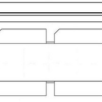
Page 10
... Note 1. millimeter dimensions are derived from the original inch dimensions. Outline version IEC SOT539B Fig 14. Package outline SOT539B BLF7G20L-250P_7G20LS-250P Product data sheet BLF7G20L-250P; BLF7G20LS-250P scale ...
Page 11
... Table 11. Revision history Document ID BLF7G20L-250P_7G20LS-250P v.3 20110103 Modifications: BLF7G20L-250P_7G20LS-250P v.2 20100909 BLF7G20L-250P_7G20LS-250P v.1 20091216 BLF7G20L-250P_7G20LS-250P Product data sheet BLF7G20L-250P; BLF7G20LS-250P Abbreviations Description Third Generation Partnership Project Complementary Cumulative Distribution Function Continuous Wave Dedicated Physical CHannel ElectroStatic Discharge Laterally Diffused Metal-Oxide Semiconductor ...
Page 12
... BLF7G20L-250P_7G20LS-250P Product data sheet BLF7G20L-250P; BLF7G20LS-250P [3] Definition This document contains data from the objective specification for product development. This document contains data from the preliminary specification. ...
Page 13
... For sales office addresses, please send an email to: BLF7G20L-250P_7G20LS-250P Product data sheet BLF7G20L-250P; BLF7G20LS-250P NXP Semiconductors’ specifications such use shall be solely at customer’s own risk, and (c) customer fully indemnifies NXP Semiconductors for any liability, damages or failed product claims resulting from customer design and use of the product for automotive applications beyond NXP Semiconductors’ ...
Page 14
... Trademarks Contact information Contents . . . . . . . . . . . . . . . . . . . . . . . . . . . . . . 14 BLF7G20L-250P; BLF7G20LS-250P Please be aware that important notices concerning this document and the product(s) described herein, have been included in section ‘Legal information’. © NXP B.V. 2011. For more information, please visit: http://www.nxp.com For sales office addresses, please send an email to: salesaddresses@nxp.com Power LDMOS transistor All rights reserved ...