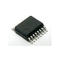
CM2006-02QR ON Semiconductor, CM2006-02QR Datasheet - Page 5

CM2006-02QR
Manufacturer Part Number
CM2006-02QR
Description
IC VGA PORT COMPANION 16QSOP
Manufacturer
ON Semiconductor
Series
Praetorian®r
Type
The CM2006 connects between the VGA or DVI-I port connector and the internal analog or digital flat panel controller logic.r
Specifications of CM2006-02QR
Applications
Monitors, TV
Voltage - Supply
5V
Package / Case
16-QSOP
Mounting Type
Surface Mount
Operating Supply Voltage
- 0.5 V to + 6 V
Supply Current
10 uA
Maximum Operating Temperature
+ 85 C
Minimum Operating Temperature
- 40 C
Mounting Style
SMD/SMT
Number Of Channels
7
Lead Free Status / RoHS Status
Lead free / RoHS Compliant
Interface
-
Lead Free Status / Rohs Status
Lead free / RoHS Compliant
Available stocks
Company
Part Number
Manufacturer
Quantity
Price
Part Number:
CM2006-02QR
Manufacturer:
CMD
Quantity:
20 000
CM2006
SYMBOL PARAMETER
I
BACKDRIVE
I
C
V
CC_DDC
R
V
V
t
V
V
V
V
I
t
t
V
I
V
IN_VID
R,
I
OFF
PLH
PHL
ESD1
CC
HYS
OUT
ESD
IN
OH
ON
OL
IH
IL
F
t
F
Note 1: All parameters specified over standard operating conditions unless otherwise noted.
Note 2: These parameters apply only to the SYNC drivers. Note that R
Note 3: Per the IEC-61000-4-2 International ESD Standard, Level 4 contact discharge method. BYP and V
Note 4: This specification applies to the SYNC_OUT pins only.
Note 5: Applicable pins are: VIDEO_1, VIDEO_2, VIDEO_3, SYNC_IN1, SYNC_IN2, DDC_IN1 and DDC_IN2.
V
V
ESD Diode Forward Voltage
Logic High Input Voltage
Logic Low Input Voltage
Hysteresis Voltage
Logic High Output Voltage
Logic Low Output Voltage
SYNC Driver Output Resistance
Input Current
Level Shifting N-MOSFET "OFF" State
Leakage Current
Current conducted from input pins when Vcc
is powered down.
Voltage Drop Across Level-shifting
N-MOSFET when "ON"
VIDEO Input Capacitance
SYNC Driver L => H Propagation Delay
SYNC Driver H => L Propagation Delay
SYNC Driver Output Rise & Fall Times
ESD Withstand Voltage, Sync_out pins only V
ESD Withstand Voltage
CC_DDC
CC
Supply Current
VIDEO Inputs
SYNC_IN1, SYNC_IN2 Inputs
GND via a low impedance ground plane with a 0.22µF, low inductance, chip ceramic capacitor at each supply pin. ESD
pulse is applied between the applicable pins and GND. ESD pulses can be positive or negative with respect to GND.
Applicable pins are: VIDEO_1, VIDEO_2, VIDEO_3, SYNC_IN1, SYNC_IN2, DDC_IN1 and DDC_IN2. All pins are ESD
protected to the industry standard ±2kV Human Body Model (MIL-STD-883, Method 3015).
Supply Current
ELECTRICAL OPERATING CHARACTERISTICS
Rev.2 | Page 5 of 9 | www.onsemi.com
CONDITIONS
V
V
SYNC outputs unloaded
V
SYNC outputs unloaded
I
V
V
V
I
I
V
V
V
(V
(V
V
V
V
V
C
C
C
V
F
OH
OL
CC_DDC
CC
CC
CC
CC
CC
CC
CC
CC
CC
CC_DDC
CC
CC
CC
CC
L
L
L
= 10mA
CC_DDC
CC_DDC
= 0mA, V
= 50pF; V
= 50pF; V
= 50pF; V
= 0mA, V
= 5V; SYNC inputs at GND or V
= 5V; SYNC inputs at 3.0V;
= 5.0V; Note 2
= 5.0V; Note 2
= 5.0V; Note 2
= 5.0V; SYNC Inputs at GND or 3.0V
= 5.0V; V
= 5.0V; V
< V
= 5.0V; V
= 2.5V; V
= 5V; Notes 3 and 4
= 5V; Notes 3 and 5
= 5.0V
= 2.5V; V
- V
- V
INPUT_PIN ;
DDC_IN
DDC_OUT
CC
CC
CC
CC
CC
IN
IN
IN
IN
Note 5
) 0.4V; V
= 5.0V; Note 2
= 5.0V; Note 2
= V
= V
= 2.5V; f = 1MHz
= 1.25V; f = 1MHz
= 5.0V; Input t
= 5.0V; Input t
= 5.0V; Input t
) 0.4V; V
S
= GND; I
CC
CC
or GND
or GND
OUT
DDC_OUT
= R
DDC_IN
DS
T
= 3mA;
R
R
R
+ R
= V
= V
and t
and t
and t
BUFFER
CC_DDC
CC_DDC
F
F
F
CC
;
5ns
5ns
.
5ns
(SEE NOTE 1)
MIN
2.0
4.0
±2
±8
7
CC
must be bypassed to
TYP
400
15
10
3
MAX UNITS
0.15
0.18
2.0
1.0
0.5
±10
±10
3.5
10
24
10
10
12
12
1
3
mA
mA
mV
µA
µA
µA
µA
µA
µA
kV
kV
pF
pF
ns
ns
ns
Ω
V
V
V
V
V
V


