VDRIVE2 FTDI, VDRIVE2 Datasheet - Page 4
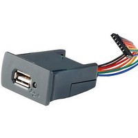
VDRIVE2
Manufacturer Part Number
VDRIVE2
Description
Interface Modules & Development Tools USB Flash Drive Interface Module
Manufacturer
FTDI
Datasheet
1.VDRIVE2.pdf
(8 pages)
Specifications of VDRIVE2
Interface Type
USB, Serial, UART, SPI
Data Bus Width
Serial, 8 bit
Operating Supply Voltage
5 V
Product
Interface Modules
For Use With/related Products
VNC1L
Lead Free Status / RoHS Status
Lead free / RoHS Compliant


Ta�le 3 - Data and Control ��us �ignal Mode �ptions - ��I Inter�ace
Figure 2 - ��I �lave Data �ead Cycle
From �tart - ��I C� must �e held high �or the entire read cycle�� and must �e ta�en low �or at least one cloc� period
aft�r th� r�ad i� co��p��t�d. Th� fir�t bit on S��I Data In i� th� R/W bit - inp�tting a ‘1’ h�r� a��o�� data to b� r�ad fro��
the chip. The ne�t �it is the address �it�� �DD�� which is used to indicate whether the data register (�0�) or the status
register (�1�) is read �rom. During the ��I read cycle a �yte o� data will start �eing output on ��I Data �ut on the ne�t
c�ock cyc�� aft�r th� addr��� bit�� MSB fir�t. �ft�r th� data ha� b��n c�ock�d o�t of th� chip�� th� �tat�� of S��I Data
�ut should �e chec�ed to see i� the data read is new data. � �0� level here on ��I Data �ut means that the data read
is new data. � �1� indicates that the data read is old data�� and the read cycle should �e repeated to get new data.
�emem�er that C� must �e held low �or at least one cloc� period �e�ore �eing ta�en high again to continue with the
ne�t read or write cycle.
Figure 3 - ��I �lave Data Write Cycle
From �tart - ��I C� must �e held high �or the entire write cycle�� and must �e ta�en low �or at least one cloc� period
aft�r th� �rit� i� co��p��t�d. Th� fir�t bit on S��I Data In i� th� R/W bit - inp�tting a ‘0’ h�r� a��o�� data to b� �ritt�n
to the chip. The ne�t �it is the address �it�� �DD�� which is used to indicate whether the data register (�0�) or the status
register (�1�) is written to. During the ��I write cycle a �yte o� data can �e input to ��I Data In on the ne�t cloc� cycle
aft�r th� addr��� bit�� MSB fir�t. �ft�r th� data ha� b��n c�ock�d in to th� chip�� th� �tat�� of S��I Data O�t �ho��d b�
VDrive2 Vinculum VNC1L Module
SPI Data Out
SPI Data Out
Datasheet Version 0.99
Pin No.
�
4
2
6
SPI Data In
SPI Data In
SPI CS
SPI CS
SPICLK
SPICLK
2.3 SPI Interface Signal Descriptions and Timing Diagrams
Name
�CLK
�DI
�D�
C�
1
Type
Input
Input
�utput
Input
1
R/W ADD
0
R/W ADD
1
0
Description
��I Cloc� input�� 12MHz ma�imum.
��I �erial Data Input
��I �erial Data �utput
��I Chip �elect Input
0
D7
D7
D6
D5
D6
D4
D5
D3
D4
D2
D3
D1
D2
D0
© Future Technology Devices International Ltd. 2007
D1
D0
Page
Related parts for VDRIVE2
Image
Part Number
Description
Manufacturer
Datasheet
Request
R

Part Number:
Description:
Interface Modules & Development Tools USB to Serial UART MiniB Dev Mod FT232R
Manufacturer:
FTDI
Datasheet:

Part Number:
Description:
BOARD, EVALUATION, EU PSU
Manufacturer:
FTDI
Datasheet:
Part Number:
Description:
BOARD, EVALUATION, UK PSU
Manufacturer:
FTDI
Datasheet:
Part Number:
Description:
BOARD, EVALUATION, US PSU
Manufacturer:
FTDI
Datasheet:
Part Number:
Description:
Specifications: Manufacturer: FTDI ; Product Category: USB Interface IC ; RoHS: Details ; Operating Supply Voltage: 3 V to 5.25 V ; Supply Current: 25 mA ; Maximum Operating Temperature: + 70 C ; Mounting Style: SMD/SMT ; Package / Case: QFN-32
Manufacturer:
FTDI
Part Number:
Description:
integr. usb2.0/uart lqfp32 rohs ftdi reel c1k...
Manufacturer:
FTDI
Datasheet:
Part Number:
Description:
Interface Development Tools USB to UART Breakout Board
Manufacturer:
FTDI
Datasheet:

Part Number:
Description:
IC USB TO SERIAL UART 32-QFN
Manufacturer:
FTDI, Future Technology Devices International Ltd

Part Number:
Description:
USB Interface IC USB to Serial UART Enhanced IC SSOP-28
Manufacturer:
FTDI
Datasheet:

Part Number:
Description:
IC, USB UART INTERFACE, SSOP-28
Manufacturer:
FTDI
Datasheet:

Part Number:
Description:
IC, USB UART INTERFACE, QFN-32
Manufacturer:
FTDI
Datasheet:
Part Number:
Description:
IC, USB FIFO INTERFACE, SSOP-28
Manufacturer:
FTDI
Datasheet:
Part Number:
Description:
MODULE, USB, 4 PORT, FT4232H BASED
Manufacturer:
FTDI
Datasheet:
Part Number:
Description:
357-036-542-201 CARDEDGE 36POS DL .156 BLK LOPRO
Manufacturer:
FTDI
Datasheet:
Part Number:
Description:
357-036-542-201 CARDEDGE 36POS DL .156 BLK LOPRO
Manufacturer:
FTDI
Datasheet: