V2DIP2-32 FTDI, V2DIP2-32 Datasheet - Page 11
V2DIP2-32
Manufacturer Part Number
V2DIP2-32
Description
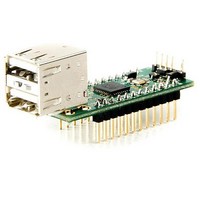
Interface Modules & Development Tools USB Vinculum-II 32 Pin Mod 2 USB Ports
Manufacturer
FTDI
Datasheet
1.V2DIP2-32.pdf
(20 pages)
Specifications of V2DIP2-32
Interface Type
USB, Serial, UART, FIFO, SPI
Data Bus Width
Serial, 8 bit
Operating Supply Voltage
5 V
Product
Interface Modules
For Use With/related Products
VNC2-32
Lead Free Status / RoHS Status
Lead free / RoHS Compliant


3.6 Parallel FIFO Interface - Asynchronous Mode
The Parallel FIFO Asynchronous mode is functionally the same as the Parallel FIFO Interface present in
VDIP1 has an eight bit data bus, individual read and write strobes and two hardware flow control signals.
3.6.1 Signal Description - Parallel FIFO Interface
The Parallel FIFO Interface signals can be programmed to a choice of available I/O pins.
shows the Parallel FIFO Interface signals and the pins that they can be mapped.
J2-10, J1-6, J1-11
J2-9, J1-8, J1-12
J2-8, J1-9, J2-12
J2-6, J1-10, J2-11
J2-10, J1-6, J1-11
J2-9, J1-8, J1-12
J2-8, J1-9, J2-12
J2-6, J1-10, J2-11
J2-10, J1-6, J1-11
J2-9, J1-8, J1-12
J2-8, J1-9, J2-12
J2-6, J1-10, J2-11
Table 3.6 - Data and Control Bus Signal Mode Options – Parallel FIFO Interface
Available Pins
Copyright © 2010 Future Technology Devices International Limited
`
fifo_data[0]
fifo_data[1]
fifo_data[2]
fifo_data[3]
fifo_data[4]
fifo_data[5]
fifo_data[6]
fifo_data[7]
fifo_txe#
fifo_rxf#
fifo_wr#
fifo_rd#
V2DIP2-32 VNCL2-32Q Development Module Datasheet Version 1.0
Name
Output
Output
Type
Input
Input
I/O
I/O
I/O
I/O
I/O
I/O
I/O
I/O
When high, do not read data from
the FIFO. When low, there is data
available in the FIFO which can be
read by strobing RD# low, then high.
When high, do not write data into the
FIFO. When low, data can be written
into the FIFO by strobing WR high,
then low.
Enables the current FIFO data byte
on D0...D7 when low. Fetches the
next FIFO data byte (if available)
from the receive FIFO buffer when
RD# goes from high to low
Writes the data byte on the D0...D7
pins into the transmit FIFO buffer
when WR goes from high to low.
Document Reference No.: FT_000164
FIFO data bus Bit 0
FIFO data bus Bit 1
FIFO data bus Bit 2
FIFO data bus Bit 3
FIFO data bus Bit 4
FIFO data bus Bit 5
FIFO data bus Bit 6
FIFO data bus Bit 7
Description
Clearance No.: FTDI# 151
Table 3.6
10
Related parts for V2DIP2-32
Image
Part Number
Description
Manufacturer
Datasheet
Request
R

Part Number:
Description:
MOD MCU-USB HOST CTLR 40-DIP
Manufacturer:
FTDI, Future Technology Devices International Ltd
Datasheet:

Part Number:
Description:
MOD MCU-USB HOST CTLR 60-DIP
Manufacturer:
FTDI, Future Technology Devices International Ltd
Datasheet:

Part Number:
Description:
BOARD, EVALUATION, UK PSU
Manufacturer:
FTDI
Datasheet:
Part Number:
Description:
BOARD, EVALUATION, US PSU
Manufacturer:
FTDI
Datasheet:
Part Number:
Description:
Specifications: Manufacturer: FTDI ; Product Category: USB Interface IC ; RoHS: Details ; Operating Supply Voltage: 3 V to 5.25 V ; Supply Current: 25 mA ; Maximum Operating Temperature: + 70 C ; Mounting Style: SMD/SMT ; Package / Case: QFN-32
Manufacturer:
FTDI
Part Number:
Description:
integr. usb2.0/uart lqfp32 rohs ftdi reel c1k...
Manufacturer:
FTDI
Datasheet:
Part Number:
Description:
Interface Development Tools USB to UART Breakout Board
Manufacturer:
FTDI
Datasheet:

Part Number:
Description:
IC USB TO SERIAL UART 32-QFN
Manufacturer:
FTDI, Future Technology Devices International Ltd

Part Number:
Description:
USB Interface IC USB to Serial UART Enhanced IC SSOP-28
Manufacturer:
FTDI
Datasheet:

Part Number:
Description:
IC, USB UART INTERFACE, SSOP-28
Manufacturer:
FTDI
Datasheet:

Part Number:
Description:
IC, USB UART INTERFACE, QFN-32
Manufacturer:
FTDI
Datasheet:
Part Number:
Description:
IC, USB FIFO INTERFACE, SSOP-28
Manufacturer:
FTDI
Datasheet:
Part Number:
Description:
MODULE, USB, 4 PORT, FT4232H BASED
Manufacturer:
FTDI
Datasheet:
Part Number:
Description:
357-036-542-201 CARDEDGE 36POS DL .156 BLK LOPRO
Manufacturer:
FTDI
Datasheet:
Part Number:
Description:
357-036-542-201 CARDEDGE 36POS DL .156 BLK LOPRO
Manufacturer:
FTDI
Datasheet: