VNCLO-SHLD-1A FTDI, VNCLO-SHLD-1A Datasheet - Page 25
VNCLO-SHLD-1A
Manufacturer Part Number
VNCLO-SHLD-1A
Description
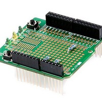
Interface Modules & Development Tools Vinculo Prototyping Shield Accessory
Manufacturer
FTDI
Datasheet
1.VNCLO-MB1A.pdf
(26 pages)
Specifications of VNCLO-SHLD-1A
Interface Type
USB, Serial, UART, FIFO, SPI
Data Bus Width
Serial, 8 bit
Operating Supply Voltage
100 VAC to 240 VAC
Product
Interface Development Tools
Features
Precompiled Drivers For A Variety Of Interfaces
Kit Contents
Board
Kit Features
Precompiled Drivers, Compatible With Existing Shields
Mcu Supported Families
VNC2
Silicon Family Name
Vinculum
For Use With/related Products
VNC2
Lead Free Status / RoHS Status
Lead free / RoHS Compliant


Document Reference No.: FT_000327
Vinco Development Module Datasheet Version 2.0
Clearance No.: FTDI#173
Appendix B – List of Figures and Tables
List of Figures
Figure 1.1 – VINCO ....................................................................................................................... 1
Figure 3.1 – Vinco Diagram ............................................................................................................ 4
Figure 8.1 – Vinco Dimensions ..................................................................................................... 15
Figure 8.2 – Vinco Pitch Measurements ......................................................................................... 15
Figure 9.1 – Vinco Schematics ...................................................................................................... 16
Figure 10.1 – Vinco_Proto ............................................................................................................ 17
List of Tables
Table 1.1 – Vinco Part Numbers ...................................................................................................... 3
Table 3.1 – Vinco Connector Descriptions ........................................................................................ 4
Table 3.2 – Pin Signal Descriptions ................................................................................................. 6
Table 3.3 – USB Slave Pin Out ........................................................................................................ 7
Table 3.4 – USB Slave Pin Out ........................................................................................................ 7
Table 3.5 – Jumper Options ........................................................................................................... 8
Table 4.1 – Data and Control Bus Signal Mode Options – UART........................................................... 9
Table 4.2 – Data and Control Bus Signal Mode Options – SPI Slave ................................................... 10
Table 4.3 – Data and Control Bus Signal Mode Options – SPI Master ................................................. 10
Table 4.4 – Data and Control Bus Signal Mode Options – Parallel FIFO Interface ................................. 11
Table 5.1 – Signal Name and Description – Debugger Interface ........................................................ 12
Table 6.1 – ADC Interface ............................................................................................................ 13
Copyright © 2010-2011 Future Technology Devices International Limited
21
Related parts for VNCLO-SHLD-1A
Image
Part Number
Description
Manufacturer
Datasheet
Request
R

Part Number:
Description:
POWER SUPPLY FOR VNCLO-MB1A USA
Manufacturer:
FTDI, Future Technology Devices International Ltd
Datasheet:

Part Number:
Description:
POWER SUPPLY FOR VNCLO-MB1A EU
Manufacturer:
FTDI, Future Technology Devices International Ltd
Datasheet:
Part Number:
Description:
POWER SUPPLY FOR VNCLO-MB1A UK
Manufacturer:
FTDI, Future Technology Devices International Ltd
Datasheet:

Part Number:
Description:
Interface Modules & Development Tools Vinculo Motherboard Req VNC2DEBUGMODULE
Manufacturer:
FTDI
Datasheet:
Part Number:
Description:
KIT, DEV, VINCULUM-II, VNC2
Manufacturer:
FTDI
Datasheet:
Part Number:
Description:
BOARD, EVALUATION, US PSU
Manufacturer:
FTDI
Datasheet:
Part Number:
Description:
Specifications: Manufacturer: FTDI ; Product Category: USB Interface IC ; RoHS: Details ; Operating Supply Voltage: 3 V to 5.25 V ; Supply Current: 25 mA ; Maximum Operating Temperature: + 70 C ; Mounting Style: SMD/SMT ; Package / Case: QFN-32
Manufacturer:
FTDI

Part Number:
Description:
IC USB TO SERIAL UART 32-QFN
Manufacturer:
FTDI, Future Technology Devices International Ltd

Part Number:
Description:
USB Interface IC USB to Serial UART Enhanced IC SSOP-28
Manufacturer:
FTDI
Datasheet:

Part Number:
Description:
IC, USB UART INTERFACE, SSOP-28
Manufacturer:
FTDI
Datasheet:

Part Number:
Description:
IC, USB UART INTERFACE, QFN-32
Manufacturer:
FTDI
Datasheet:
Part Number:
Description:
IC, USB FIFO INTERFACE, SSOP-28
Manufacturer:
FTDI
Datasheet:
Part Number:
Description:
MODULE, USB, 4 PORT, FT4232H BASED
Manufacturer:
FTDI
Datasheet:
Part Number:
Description:
357-036-542-201 CARDEDGE 36POS DL .156 BLK LOPRO
Manufacturer:
FTDI
Datasheet:
Part Number:
Description:
357-036-542-201 CARDEDGE 36POS DL .156 BLK LOPRO
Manufacturer:
FTDI
Datasheet: