V2DIP2-48 FTDI, V2DIP2-48 Datasheet
V2DIP2-48
Specifications of V2DIP2-48


Related parts for V2DIP2-48


V2DIP2-48 Summary of contents
Page 1
... No freedom to use patents or other intellectual property rights is implied by the publication of this document. Future Technology Devices International Ltd, Unit 1, 2 Seaward Place, Centurion Business Park, Glasgow, G41 1HH, United Kingdom. Scotland Registered Number: SC136640 Copyright © 2010 Future Technology Devices International Limited V2DIP2-48 Datasheet Document Reference No.: FT_000237 Version 1.01 ...
Page 2
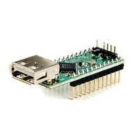
... Introduction V2DIP2-48 module is designed to allow rapid development of designs using the VNC2-48Q IC. The V2DIP1-48 is supplied as a PCB designed provides access to the UART, parallel FIFO, and SPI interface pins of the VNC2-48Q device, via its IO bus pins. Two USB ports are accessed via type A USB connectors. ...
Page 3
... Contact Information............................................................................. 21 Appendix A – References ............................................................................................ 22 Appendix B– List of Figures and Tables .................................................................... 23 List of Figures............................................................................................................... 23 List of Tables ................................................................................................................ 23 Appendix C – Revision History ................................................................................... 24 Copyright © 2010 Future Technology Devices International Limited V2DIP2-48 VNC2-48 Development Module Datasheet Version 1.01 Table of Contents Document Reference No.: FT_000237 Clearance No.: FTDI# 152 2 ...
Page 4
... Auxiliary 3 200 mA power output to external logic. Copyright © 2010 Future Technology Devices International Limited Document Reference No.: FT_000237 V2DIP2-48 VNC2-48 Development Module Datasheet Version 1.01 : All VNC2 signals available on 0.6” wide. 0.1” pitch DIL male connectors. Power and traffic indicator LED’s V2DIP2- Pb-free, RoHS complaint development module ...
Page 5
... Pin Out and Signal Description 3.1 Module Pin Out Figure 3.1 - V2DIP2 48 Module Pin Out (Top View) Copyright © 2010 Future Technology Devices International Limited Document Reference No.: FT_000237 V2DIP2-48 VNC2-48 Development Module Datasheet Version 1.01 Clearance No.: FTDI# 152 4 ...
Page 6
... Figure 3.2 - V2DIP2 48 Module Pin Out (Bottom View) Copyright © 2010 Future Technology Devices International Limited Document Reference No.: FT_000237 V2DIP2-48 VNC2-48 Development Module Datasheet Version 1.01 Clearance No.: FTDI# 152 5 ...
Page 7
... PWR 5.0V module supply pin. This pin can be used to provide the 5.0V input to the V2DIP2-48 when the V2DIP2-48 is not powered from the USB connector (VBUS) or the debugger interface. Also connected to DIL connector pins J1-2, J1-3 and J1-9 and J3-6. ...
Page 8
... Not Connected PWR 3.3V output from V2DIP2-48 on board 3.3V L.D.O. Output PWR 3.3V output from V2DIP2-48 on board 3.3V L.D.O. Output I/O 5V safe bidirectional data / control bus bit 4 I/O 5V safe bidirectional data / control bus bit 3 I/O ...
Page 9
... NOTE: This is only applicable when using VNC1L compatible firmware e.g. V2DAP2. Other wise the user can set the pins for their own use. Copyright © 2010 Future Technology Devices International Limited Document Reference No.: FT_000237 V2DIP2-48 VNC2-48 Development Module Datasheet Version 1.01 Figure 3.3 IOBUS26 (VNC2-48Q pin 46) ...
Page 10
... IO18 J2-19 IOBUS19 IO19 J2-18 IOBUS20 IO20 Table 3.3 - Default Interface I/O Pin Configuration Copyright © 2010 Future Technology Devices International Limited V2DIP2-48 VNC2-48 Development Module Datasheet Version 1.01 Data and Control Bus Configuration UART SPI Slave Interface Interface NA NA I/O ...
Page 11
... J2-5, JI-6, J1-11, J1-18, J2-19, J2-14 J2-8, J2-4, J1-7, J1-14, J1-19, J2-18, J2-13 Table 3.4 - Data and Control Bus Signal Mode Options – UART Interface Copyright © 2010 Future Technology Devices International Limited V2DIP2-48 VNC2-48 Development Module Datasheet Version 1.01 Name Type uart_txd Output uart_rxd# ...
Page 12
... J2-5, JI-6, J1-11, J1-18, J2-19, J2-14 J2-8, J2-4, J1-7, J1-14, J1-19, J2-18, J2-13 Table 3.6 - Data and Control Bus Signal Mode Options – SPI Master Copyright © 2010 Future Technology Devices International Limited V2DIP2-48 VNC2-48 Development Module Datasheet Version 1.01 FTDI website. Name Type spi_s0_clk ...
Page 13
... J2-6, J1-5, J1-10, J1-17, J2-20, J2-16 J2-5, JI-6, J1-11, J1-18, J2-19, J2-14 Table 3.7 - Data and Control Bus Signal Mode Options – Parallel FIFO Interface Copyright © 2010 Future Technology Devices International Limited V2DIP2-48 VNC2-48 Development Module Datasheet Version 1.01 Name Type I/O ...
Page 14
... When FIFO_WR# goes low FIFO_TXE# flag will always go high. FIFO_TXE# goes low again only when there is still space for data to be written in to the module. Copyright © 2010 Future Technology Devices International Limited Document Reference No.: FT_000237 V2DIP2-48 VNC2-48 Development Module Datasheet Version 1.01 Min Max Unit ...
Page 15
... J2-7, J1-4, J1-8, J1-16, J1-20, J2-17 Table 3.9 - Data and Control Bus Signal Mode Options – Synchronous FIFO mode Copyright © 2010 Future Technology Devices International Limited Document Reference No.: FT_000237 V2DIP2-48 VNC2-48 Development Module Datasheet Version 1.01 Name Type Output fifo_oe# ...
Page 16
... Write DATA hold time t13 WR# setup time t14 WR# hold time Table 3.10 - Synchronous FIFO Mode Read and Write Cycle Timing Copyright © 2010 Future Technology Devices International Limited Document Reference No.: FT_000237 V2DIP2-48 VNC2-48 Development Module Datasheet Version 1.01 Min Typical Max Uni - 20. ...
Page 17
... Similarly when bursts of data are to be written to the module WR# should be kept low. TXE# remains low when there is still space available for the data to be written Copyright © 2010 Future Technology Devices International Limited Document Reference No.: FT_000237 V2DIP2-48 VNC2-48 Development Module Datasheet Version 1.01 Clearance No.: FTDI# 152 16 ...
Page 18
... PRG# J3-5 J3-6 5V0 VCC Table 3.11 - Signal Name and Description – Debugger Interface Copyright © 2010 Future Technology Devices International Limited V2DIP2-48 VNC2-48 Development Module Datasheet Version 1.01 Type Description I/O Debugger Interface - Not connected. Used to make sure that the debug module is connected correctly ...
Page 19
... Firmware 4.1 Firmware Support The VNC2 on the V2DIP2-48 can be programmed with the customers own firmware created using the Vinculum II firmware development tool chain or with various pre-compiled firmware profiles to allow a designer to easily change the functionality of the chip. Please refer to:- available pre-compiled firmware 4 ...
Page 20
... Figure 5.1 V2DIP2 48 Dimensions (Top View) Figure 5.2 V2DIP2 48 Dimensions (Side View) Tolerance is ±0.20mm All dimensions are in mm Copyright © 2010 Future Technology Devices International Limited Document Reference No.: FT_000237 V2DIP2-48 VNC2-48 Development Module Datasheet Version 1.01 68.56 59.70 60.96 2.54 Clearance No.: FTDI# 152 ...
Page 21
... Schematic Diagram Figure 6.1 - Schematic Diagram Copyright © 2010 Future Technology Devices International Limited Document Reference No.: FT_000237 V2DIP2-48 VNC2-48 Development Module Datasheet Version 1.01 Clearance No.: FTDI# 152 20 ...
Page 22
... Please visit the Sales Network page of the FTDI Web site for the contact details of our distributor(s) and sales representative(s) in your country. Copyright © 2010 Future Technology Devices International Limited Document Reference No.: FT_000237 V2DIP2-48 VNC2-48 Development Module Datasheet Version 1.01 Clearance No.: FTDI# 152 21 ...
Page 23
... Vinculum-II Debug Interface Description Vinculum-II IO Mux Explained Vinculum-II PWM Example Migrating Vinculum Designs From VNC1L to VNC2-48L1A Vinculum-II Errata Technical Note Copyright © 2010 Future Technology Devices International Limited Document Reference No.: FT_000237 V2DIP2-48 VNC2-48 Development Module Datasheet Version 1.01 Clearance No.: FTDI# 152 22 ...
Page 24
... Table 3.9 - Data and Control Bus Signal Mode Options – Synchronous FIFO mode .............................. 14 Table 3.10 - Synchronous FIFO Mode Read and Write Cycle Timing ................................................... 15 Table 3.11 - Signal Name and Description – Debugger Interface ....................................................... 17 Copyright © 2010 Future Technology Devices International Limited Document Reference No.: FT_000237 V2DIP2-48 VNC2-48 Development Module Datasheet Version 1.01 Clearance No.: FTDI# 152 23 ...
Page 25
... Version 1.0 First Release Version 1.01 Added module’s images and edited mechanical drawings Copyright © 2010 Future Technology Devices International Limited Document Reference No.: FT_000237 V2DIP2-48 VNC2-48 Development Module Datasheet Version 1.01 Clearance No.: FTDI# 152 16th April 2010 25th May 2010 24 ...