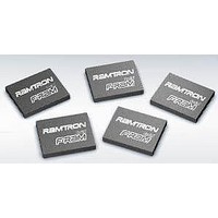
FM25H20-DG Ramtron, FM25H20-DG Datasheet

FM25H20-DG
Specifications of FM25H20-DG
Available stocks
Related parts for FM25H20-DG
FM25H20-DG Summary of contents
Page 1
... TDFN Package • 8- pin “Green”/RoHS EIAJ SOIC Package Pin Configuration VSS VSS Pinout is equivalent to other SPI F-RAM devices. Pin Name /S /W /HOLD VDD VSS Ordering Information FM25H20-DG FM25H20-DGTR FM25H20-G FM25H20-GTR Top View /S VDD /HOLD VDD 1 ...
Page 2
... Q may be connected to D for a single pin data interface. VDD Supply Power Supply (2.7V to 3.6V) VSS Supply Ground Rev. 2.2 Sept. 2010 18 Counter Data I/O Register Nonvolatile Status Figure 1. Block Diagram specifications. DD FM25H20 - 2Mb SPI FRAM 32768 x 64 FRAM Array Register Page ...
Page 3
... For both modes, data is clocked into the FM25H20 on the rising edge of C and data is expected on the first rising edge after /S goes active. If the clock starts from a high state, it will fall prior to the first data transfer in order to create the first rising edge ...
Page 4
... Figure 2. 512KB System Configuration with SPI port Figure 3. System Configuration without SPI port SPI Mode 0: CPOL=0, CPHA=0 SPI Mode 3: CPOL=1, CPHA=1 Rev. 2.2 Sept. 2010 Figure 4. SPI Modes 0 & 3 FM25H20 - 2Mb SPI FRAM Page ...
Page 5
... Power Up to First Access The FM25H20 is not accessible for a period of time (1 ms) after power up. Users must comply with the timing parameter t , which is the minimum time PU from V (min) to the first /S low. DD Data Transfer All data transfers to and from the FM25H20 occur in 8-bit groups. They are synchronized to the clock signal (C), and they transfer most significant bit (MSB) first ...
Page 6
... Status Register. Reading Status provides information about the current state of the write protection features. Following the RDSR op- code, the FM25H20 will return one byte with the contents of the Status Register. The Status Register is described in detail in the section below. ...
Page 7
... The SPI interface, which is capable of a relatively high clock frequency, highlights the fast write capability of the F-RAM technology. Unlike Serial Flash, the FM25H20 can perform sequential writes at bus speed. No page buffer is needed and any number of sequential writes may be performed. Write Operation All writes to the memory array begin with a WREN op-code ...
Page 8
... Q Sleep Mode A low power mode called Sleep Mode is implemented on the FM25H20. The device will enter this low power state when the SLEEP op-code (B9h) is clocked in, and the device seeing the rising edge of /S. Once in sleep mode, the C and D pins are ignored and Q will hi-Z state, but the device continues to monitor the /S pin ...
Page 9
... Endurance The FM25H20 is capable of being accessed at least 14 10 times, reads or writes. An F-RAM memory operates with a read and restore mechanism. Therefore, an endurance cycle is applied on a row basis for each access (read or write) to the memory array. The F-RAM architecture is based on an array of rows and columns. Rows are defined by A17-A3 and column addresses by A2-A0 ...
Page 10
... DD Min Typ 2.7 3 -0.4 0 – 0 other inputs -0.2V FM25H20 - 2Mb SPI FRAM Ratings -1.0V to +4.5V -1.0V to +4.5V and V < V +1. -55° 125°C 260° C 2kV 1kV 200V MSL-1 (TDFN) MSL-1 (EIAJ) Max Units Notes 3 1 μ A 150 μ A 270 3 μ ...
Page 11
... This parameter is characterized and not 100% tested. Data Retention (T = -40°C to +85°C) A Symbol Parameter T Data Retention DR Rev. 2.2 Sept. 2010 = 2.7V to 3.6V 30pF Min 3.3V) DD Min - - Min Units 10 Years FM25H20 - 2Mb SPI FRAM Max Units Notes 40 MHz 2 2 Max Units Notes 8 ...
Page 12
... V Rise Time Fall Time VF DD Notes 1. This parameter is characterized and not 100% tested. 2. Slope measured at any point Rev. 2.2 Sept. 2010 1 ODV min 2.7V to 3.6V) DD min) DD waveform. FM25H20 - 2Mb SPI FRAM CSH Min Max Units Notes μ μ - 450 s μ 50 ...
Page 13
... R=Ramtron, G=”green” TDFN package XXXX=base part number LLLL= lot code RGXXXX YY=year, WW=work week LLLL YYWW Example: “Green” TDFN package, FM25H20, Lot 0012, Year 2010, Work Week 10 RG5H20 0012 1010 Rev. 2.2 Sept. 2010 FM25H20 - 2Mb SPI FRAM Page ...
Page 14
... EIAJ SOIC Package Marking Scheme Legend: XXXXXX= part number LLLLLLL= lot code RIC=Ramtron Int’l Corp, YY=year, WW=work week XXXXXXX-G LLLLLLL FM25H20, “Green” EIAJ SOIC package, Year 2009, Work Week 40 RIC YYWW FM25H20-G B90003G1 RIC 0940 Rev. 2.2 Sept. 2010 Recommended PCB Footprint 5 ...
Page 15
... Added EIAJ SOIC package. Added ESD ratings. Changed recommended DFN pcb footprint. Updated lead temperature rating in Abs Max table. 2.2 9/21/2010 Modified DFN mechanical drawing and recommended pcb footprint. Date code of new package starts at 1010. Rev. 2.2 Sept. 2010 FM25H20 - 2Mb SPI FRAM , I , and I limits. Changed specs ...


