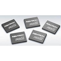
FM25H20-DG Ramtron, FM25H20-DG Datasheet - Page 7

FM25H20-DG
Manufacturer Part Number
FM25H20-DG
Description
F-RAM 2Mb (256kX8) 3V
Manufacturer
Ramtron
Datasheet
1.FM25H20-DG.pdf
(15 pages)
Specifications of FM25H20-DG
Operating Supply Voltage
2.7 V to 3.6 V
Operating Temperature Range
- 40 C to + 85 C
Mounting Style
SMD/SMT
Package / Case
DFN-8
Memory Size
2Mbit
Memory Configuration
256K X 8
Interface Type
Serial, SPI
Supply Voltage Range
2.7V To 3.6V
Memory Case Style
TDFN
No. Of Pins
8
Rohs Compliant
Yes
Ic Interface Type
Serial, SPI
Nvram Features
2 Mbit Ferroelectric Nonvolatile RAM, Low Power Consumption, Write Protection Scheme
Lead Free Status / RoHS Status
Lead free / RoHS Compliant
Available stocks
Company
Part Number
Manufacturer
Quantity
Price
Company:
Part Number:
FM25H20-DG
Manufacturer:
RAMTRON
Quantity:
1 260
Company:
Part Number:
FM25H20-DGTR
Manufacturer:
ATMEL
Quantity:
13 400
Bits 0, 4, 5 are fixed at 0 and bit 6 is fixed at 1, and
none of these bits can be modified. Note that bit 0
(“Write in Progress” bit in Serial Flash) is
unnecessary as the F-RAM writes in real-time and is
never busy, so it reads out as a ‘0’. There is an
exception to this when the device is waking up from
Sleep Mode, which is described on the following
page.
protection features. They are nonvolatile (shaded
yellow). The WEL flag indicates the state of the
Write Enable Latch. Attempting to directly write the
WEL bit in the Status Register has no effect on its
state. This bit is internally set and cleared via the
WREN and WRDI commands, respectively.
BP1 and BP0 are memory block write protection bits.
They specify portions of memory that are write-
protected as shown in the following table.
Table 3. Block Memory Write Protection
Table 4. Write Protection
Memory Operation
The SPI interface, which is capable of a relatively
high clock frequency, highlights the fast write
capability of the F-RAM technology. Unlike Serial
Flash, the FM25H20 can perform sequential writes at
bus speed. No page buffer is needed and any number
of sequential writes may be performed.
Write Operation
All writes to the memory array begin with a WREN
op-code. The next op-code is the WRITE instruction.
This op-code is followed by a three-byte address
value, which specifies the 18-bit address of the first
data byte of the write operation. Note that the first 6-
bits in the most significant address byte are ignored.
Subsequent bytes are data and they are written
sequentially. Addresses are incremented internally as
long as the bus master continues to issue clocks. If
the last address of 3FFFFh is reached, the counter
will roll over to 00000h. Data is written MSB first. A
write operation is shown in Figure 9.
Rev. 2.2
Sept. 2010
BP1
0
0
1
1
WEL
0
1
1
1
The BP1 and BP0 control software write
BP0
0
1
0
1
WPEN
X
0
1
1
Protected Address Range
None
30000h to 3FFFFh (upper ¼)
20000h to 3FFFFh (upper ½)
00000h to 3FFFFh (all)
/W
X
X
0
1
Protected Blocks
Protected
Protected
Protected
Protected
The BP1 and BP0 bits and the Write Enable Latch
are the only mechanisms that protect the memory
from writes. The remaining write protection features
protect inadvertent changes to the block protect bits.
The WPEN bit controls the effect of the hardware pin
/W. When WPEN=0, the /W pin is ignored. When
WPEN=1, the /W pin controls write access to the
Status Register. Thus the Status Register is write-
protected only when WPEN=1 and the /W pin is low.
This scheme provides a write protection mechanism
which can prevent software from writing the memory
under any circumstances. This occurs if the BP1 and
BP0 are set to 1, the WPEN bit is set to 1, and the /W
pin is low. This occurs because the block protect bits
prevent writing memory and the /W signal in
hardware prevents altering the block protect bits (if
WPEN is high). Therefore in this condition, hardware
must be involved in allowing a write operation. The
following table summarizes the write protection
conditions.
Unlike Serial Flash, any number of bytes can be
written sequentially and each byte is written to
memory immediately after it is clocked in (after the
8
op-code operation. Asserting /W active in the middle
of a write operation will have no effect until the next
falling edge of /S.
Read Operation
After the falling edge of /S, the bus master can issue
a READ op-code. Following this instruction is a
three-byte address value, 18-bits specifying the
address of the first data byte of the read operation.
After the op-code and address are complete, the D
line is ignored. The bus master issues 8 clocks, with
one bit read out for each. Addresses are incremented
internally as long as the bus master continues to issue
clocks. If the last address of 3FFFFh is reached, the
counter will roll over to 00000h. Data is read MSB
first. The rising edge of /S terminates a READ op-
code operation. A read operation is shown in Figure
10.
th
Unprotected Blocks
Protected
Unprotected
Unprotected
Unprotected
clock). The rising edge of /S terminates a WRITE
FM25H20 - 2Mb SPI FRAM
Status Register
Protected
Unprotected
Protected
Unprotected
Page 7 of 15


