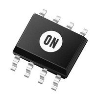
NCP3126ADR2G ON Semiconductor, NCP3126ADR2G Datasheet - Page 15

NCP3126ADR2G
Manufacturer Part Number
NCP3126ADR2G
Description
DC/DC Switching Converters 3A PWM Switching Buck Regulator
Manufacturer
ON Semiconductor
Datasheet
1.NCP3126ADR2G.pdf
(23 pages)
Specifications of NCP3126ADR2G
Mounting Style
SMD/SMT
Duty Cycle (max)
80 %
Efficiency
93 %
Input / Supply Voltage (max)
13.2 V
Input / Supply Voltage (min)
4.5 V
Maximum Operating Temperature
+ 125 C
Minimum Operating Temperature
- 40 C
Operating Temperature Range
- 40 C to + 125 C
Output Current
3 A
Output Voltage
Adjustable
Supply Current
10 mA
Switching Frequency
350 KHz
Package / Case
SOIC-8
Lead Free Status / RoHS Status
Lead free / RoHS Compliant
Available stocks
Company
Part Number
Manufacturer
Quantity
Price
Company:
Part Number:
NCP3126ADR2G
Manufacturer:
ON
Quantity:
2 500
R
R
V
V
associated standard R
Table 5. OUTPUT VOLTAGE SETTINGS
1
2
OUT
REF
The most frequently used output voltages and their
V
O
0.8
1.0
1.1
1.2
1.5
1.8
2.5
3.3
5.0
(V)
R
2
= Top resistor divider
= Bottom resistor divider
= Output voltage
= Regulator reference voltage
+ R
1
1
and R
@
R
1
2.55
3.83
4.99
12.7
21.5
31.6
52.3
1.0
V
10
(kW)
2
OUT
values are listed in Table 5.
V
REF
* V
REF
R
Open
2
10.2
11.5
10.2
10
10
10
10
10
(kW)
(eq. 39)
http://onsemi.com
15
Transconductance Error Amplifier can be calculated using
the method described below. The method serves to provide
a good starting place for compensation of a power supply.
The values can be adjusted in real time using the
compensation tool comp calc, available for download at
ON Semiconductor’s website.
least 2X the value of R
noise. Using the 2X assumption, R
the feed through capacitor can be calculated as shown
below:
The compensation components for the Pseudo Type III
The value of the feed through resistor should always be at
2
to minimize error from feed through
F
will be set to 20 kW and


