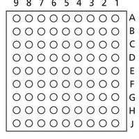
AGLN020V2-CSG81 Actel, AGLN020V2-CSG81 Datasheet - Page 33

AGLN020V2-CSG81
Manufacturer Part Number
AGLN020V2-CSG81
Description
FPGA - Field Programmable Gate Array 20K System Gates IGLOO nano
Manufacturer
Actel
Datasheet
1.AGLN030V5-ZUCG81.pdf
(140 pages)
Specifications of AGLN020V2-CSG81
Processor Series
AGLN020
Core
IP Core
Number Of Macrocells
172
Maximum Operating Frequency
250 MHz
Number Of Programmable I/os
52
Supply Voltage (max)
1.5 V
Supply Current
6 uA
Maximum Operating Temperature
+ 70 C
Minimum Operating Temperature
- 20 C
Development Tools By Supplier
AGLN-Nano-Kit, AGLN-Z-Nano-Kit, AGL-Dev-Kit-SCS, Silicon-Explorer II, Silicon-Sculptor 3, SI-EX-TCA, FLASHPRO 4, FlashPro 3, FLASHPRO LITE
Mounting Style
SMD/SMT
Supply Voltage (min)
1.2 V
Number Of Gates
20 K
Package / Case
CSP-81
Lead Free Status / RoHS Status
Lead free / RoHS Compliant
- Current page: 33 of 140
- Download datasheet (5Mb)
Table 2-21 • Summary of Maximum and Minimum DC Input and Output Levels
Table 2-22 • Summary of Maximum and Minimum DC Input Levels
I/O Standard
3.3 V LVTTL /
3.3 V LVCMOS
3.3 V LVCMOS
Wide Range
2.5 V LVCMOS
1.8 V LVCMOS
1.5 V LVCMOS
1.2 V LVCMOS
1.2 V LVCMOS
Wide Range
Notes:
1. Currents are measured at 85°C junction temperature.
2. Note that 1.2 V LVCMOS and 3.3 V LVCMOS wide range is applicable to 100 µA drive strength only. The configuration
3. All LVCMOS 3.3 V software macros support LVCMOS 3.3 V wide range, as specified in the JESD8-B specification.
4. Applicable to IGLOO nano V2 devices operating at V
5. All LVCMOS 1.2 V software macros support LVCMOS 1.2 V wide range, as specified in the JESD8-12 specification.
DC I/O Standards
3.3 V LVTTL / 3.3 V LVCMOS
3.3 V LVCOMS Wide Range
2.5 V LVCMOS
1.8 V LVCMOS
1.5 V LVCMOS
1.2 V LVCMOS
1.2 V LVCMOS Wide Range
Notes:
1. Commercial range (–20°C < T
2. Industrial range (–40°C < T
3. I
4. I
5. Applicable to IGLOO nano V2 devices operating at VCCI ≥ VCC.
will not operate at the equivalent software default drive strength. These values are for normal ranges only.
current is larger when operating outside recommended ranges.
IH
IL
is the input leakage current per I/O pin over recommended operating conditions, where –0.3 V < VIN < VIL.
is the input leakage current per I/O pin over recommended operating conditions, where VIH < VIN < VCCI. Input
3
4,5
Overview of I/O Performance
Summary of I/O DC Input and Output Levels – Default I/O Software
Settings
Applicable to Commercial and Industrial Conditions—Software Default Settings
Applicable to Commercial and Industrial Conditions
4
5
Strength
100 µA
100 µA
Drive
8 mA
8 mA
4 mA
2 mA
1 mA
Equivalent
Strength
Software
Default
5
Drive
8 mA
8 mA
8 mA
4 mA
2 mA
1 mA
1 mA
A
< 85°C)
A
< 70°C)
2
Slew
Rate
High –0.3
High –0.3
High –0.3 0.35 * VCCI 0.65 * VCCI 3.6
High –0.3 0.35 * VCCI 0.65 * VCCI 3.6 0.25 * VCCI 0.75 * VCCI
High –0.3 0.35 * VCCI 0.65 * VCCI 3.6 0.25 * VCCI 0.75 * VCCI
High –0.3 0.3 * VCCI 0.7 * VCCI 3.6
High –0.3
Min.
V
VIL
CCI
Max.
I
µA
IL
10
10
10
10
10
10
10
0.8
0.8
0.7
V
≥
R ev i si o n 1 1
3
V
Commercial
CC
.
Min.
1.7
V
2
2
VIH
1
I
IH
µA
10
10
10
10
10
10
10
Max
4
3.6
3.6
. V
3.6
IGLOO nano Low Power Flash FPGAs
Max.
VOL
0.45
0.2
0.7
0.1
0.4
V
I
µA
IL
15
15
15
15
15
15
15
3
VCCI – 0.45 4
VCCI – 0.1 100
VCCI – 0.2 100
Industrial
VOH
Min.
2.4
1.7
V
2
I
I
mA mA
µA
IH
15
15
15
15
15
15
15
OL
µA
µA
8
8
2
1
4
1
I
100
100
OH
µA
µA
2- 19
8
1
8
4
2
1
Related parts for AGLN020V2-CSG81
Image
Part Number
Description
Manufacturer
Datasheet
Request
R

Part Number:
Description:
AGLN020V2-CSG81I
Manufacturer:
Actel
Datasheet:

Part Number:
Description:
AGLN020V2-QNG68I
Manufacturer:
Actel
Datasheet:

Part Number:
Description:
AGLN020V2-UCG81I
Manufacturer:
Actel
Datasheet:

Part Number:
Description:
PBGA 81/FPGA, 520 CLBS, 20000 GATES, 250 MHz
Manufacturer:
Actel
Datasheet:

Part Number:
Description:
FPGA - Field Programmable Gate Array 20K System Gates IGLOO nano
Manufacturer:
Actel
Datasheet:

Part Number:
Description:
MCU, MPU & DSP Development Tools Silicon Sculptor Programming Mod
Manufacturer:
Actel

Part Number:
Description:
MCU, MPU & DSP Development Tools InSystem Programming ProASICPLUS Devices
Manufacturer:
Actel

Part Number:
Description:
Programming Socket Adapters & Emulators PQ160 Module
Manufacturer:
Actel

Part Number:
Description:
Programming Socket Adapters & Emulators Axcelerator Adap Module Kit
Manufacturer:
Actel

Part Number:
Description:
Programming Socket Adapters & Emulators Evaluation
Manufacturer:
Actel

Part Number:
Description:
Programming Socket Adapters & Emulators AFDX Solutions
Manufacturer:
Actel

Part Number:
Description:
Programming Socket Adapters & Emulators SILICON SCULPTOR ADAPTER MODULE
Manufacturer:
Actel
Datasheet:

Part Number:
Description:
Programming Socket Adapters & Emulators Axcelerator Adap Module Kit
Manufacturer:
Actel

Part Number:
Description:
Programming Socket Adapters & Emulators Evaluation
Manufacturer:
Actel

Part Number:
Description:
Programming Socket Adapters & Emulators Silicon Sculptor Software
Manufacturer:
Actel


