NTE312 NTE ELECTRONICS, NTE312 Datasheet

Replacement Semiconductors N-CH -30V 50mA BULK

NTE312

Manufacturer Part Number
NTE312
Description
Replacement Semiconductors N-CH -30V 50mA BULK
Manufacturer
NTE ELECTRONICS
Datasheet

Specifications of NTE312

Breakdown Voltage Vbr
-30V
Gate-source Cutoff Voltage Vgs(off) Max
-6V
Power Dissipation Pd
250mW
No. Of Pins
3
Gate-source Breakdown Voltage
-50V
Mounting Type
Through Hole
Power (ptot)
250µW
Current Rating
15mA
Rohs Compliant
Yes
Lead Free Status / RoHS Status
Lead free / RoHS Compliant
Lead Free Status / RoHS Status
Lead free / RoHS Compliant, Lead free / RoHS Compliant
Description:
The NTE312 is a field effect transistor designed for VHF amplifier and mixer applications. The
NTE312 comes in a TO–92 package.
Features:
D High Power Gain: 10dB Min at 400MHz
D High Transconductance: 4000 mho Min at 400MHz
D Low C
D High (Y
D Drain and Gate Leads Separated for High Maximum Stable Gain
D Cross–Modulation Minimized by Square–Law Transfer Characteristic
D For Use in VHF Amplifiers in FM, TV, and Mobile Communications Equipment
Absolute Maximum Ratings: (T
Drain–Gate Voltage, V
Gate–Source Voltage, V
Gate Current, I
Total Device Dissipation (T
Storage Temperature Range, T
Lead Temperature, During Soldering (1/16 Inch from Case for 10sec), T
Derate Above +25 C
Derate Above +25 C
rss
fs
: 1pF Max
) / C
G
iss
. . . . . . . . . . . . . . . . . . . . . . . . . . . . . . . . . . . . . . . . . . . . . . . . . . . . . . . . . . . . . . . . . .
Ratio (High–Frequency Figure–of–Merit)
DG
GS
. . . . . . . . . . . . . . . . . . . . . . . . . . . . . . . . . . . . . . . . . . . . . . . . . . . . . . . . . . . .
A
C
. . . . . . . . . . . . . . . . . . . . . . . . . . . . . . . . . . . . . . . . . . . . . . . . . . . . . . . . .
. . . . . . . . . . . . . . . . . . . . . . . . . . . . . . . . . . . . . . . . . . . . . . . . . . .
. . . . . . . . . . . . . . . . . . . . . . . . . . . . . . . . . . . . . . . . . . . . . . . . . . . .
= +25 C ), P
= +25 C), P
stg
N–Channel Silicon Junction
A
. . . . . . . . . . . . . . . . . . . . . . . . . . . . . . . . . . . . . . . . . .
Field Effect Transistor
= +25 C unless otherwise specified)
D
D
. . . . . . . . . . . . . . . . . . . . . . . . . . . . . . . . . . . . . . . . .
. . . . . . . . . . . . . . . . . . . . . . . . . . . . . . . . . . . . . . . . .
NTE312
L
. . . . . . . . . . . . . . .
–65 to +150 C
2.88mW/ C
4.0mW/ C
360mW
500mW
+260 C
50mA
–30V
30V

Related parts for NTE312

NTE312 Summary of contents

Page 1

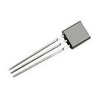
... Description: The NTE312 is a field effect transistor designed for VHF amplifier and mixer applications. The NTE312 comes in a TO–92 package. Features: D High Power Gain: 10dB Min at 400MHz D High Transconductance: 4000 mho Min at 400MHz D Low C : 1pF Max rss D High ( Ratio (High–Frequency Figure–of–Merit) ...

Page 2

Electrical Characteristics: (T Parameter OFF Characteristics Gate–Source Breakdown Voltage Gate Reverse Current Gate 1 Leakage Current Gate–Source Cutoff Voltage ON Characteristics Zero–Gate Voltage Drain Current Small–Signal Characteristics Forward Transfer Admittance Input Admittance Output Admittance Output Conductance Forward Transconductance Input Capacitance ...

Page 3

Max .500 (12.7) Min .100 (2.54) .105 (2.67) Max .205 (5.2) Max .135 (3.45) Min Seating Plane .021 (.445) Dia Max .050 (1.27) .165 (4.2) Max .105 (2.67) Max NOTE: Drain and Source are interchangeable. ...

Related keywords