DS1822+ Maxim Integrated Products, DS1822+ Datasheet - Page 7
DS1822+
Manufacturer Part Number
DS1822+
Description
Board Mount Temperature Sensors IC THERMOMETER ECONO DIG
Manufacturer
Maxim Integrated Products
Datasheet
1.DS1822Z.pdf
(21 pages)
Specifications of DS1822+
Temperature Threshold
Programmable
Full Temp Accuracy
+/- 2 C
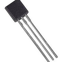
Package / Case
TO-92
Digital Output - Bus Interface
1-Wire
Digital Output - Number Of Bits
9 bit to 12 bit
Supply Voltage (max)
5.5 V
Supply Voltage (min)
3 V
Maximum Operating Temperature
+ 125 C
Minimum Operating Temperature
- 55 C
Output Type
Digital
Supply Current
1.5 mA
Ic Output Type
Digital
Sensing Accuracy Range
± 2°C
Supply Voltage Range
3V To 5.5V
Resolution (bits)
12bit
Sensor Case Style
TO-92
No. Of Pins
3
Accuracy %
2°C
Rohs Compliant
Yes
Lead Free Status / RoHS Status
Lead free / RoHS Compliant


MEMORY
The DS1822’s memory is organized as shown in Figure 7. The memory consists of an SRAM scratchpad
with NV EEPROM storage for the high and low alarm trigger registers (T
register. Note that if the DS1822 alarm function is not used, the T
purpose memory. All memory commands are described in detail in the DS1822 FUNCTION
COMMANDS section.
Byte 0 and byte 1 of the scratchpad contain the LSB and the MSB of the temperature register,
respectively. These bytes are read-only. Bytes 2 and 3 provide access to T
contains the configuration register data, which is explained in detail in the CONFIGURATION
REGISTER section of this data sheet. Bytes 5, 6, and 7 are reserved for internal use by the device and
cannot be overwritten.
Byte 8 of the scratchpad is read-only and contains the cyclic redundancy check (CRC) code for bytes 0
through 7 of the scratchpad. The DS1822 generates this CRC using the method described in the CRC
GENERATION section.
Data is written to bytes 2, 3, and 4 of the scratchpad using the Write Scratchpad [4Eh] command; the data
must be transmitted to the DS1822 starting with the least significant bit of byte 2. To verify data integrity,
the scratchpad can be read (using the Read Scratchpad [BEh] command) after the data is written. When
reading the scratchpad, data is transferred over the 1-Wire bus starting with the least significant bit of
byte 0. To transfer the T
issue the Copy Scratchpad [48h] command.
Data in the EEPROM registers is retained when the device is powered down; at power-up the EEPROM
data is reloaded into the corresponding scratchpad locations. Data can also be reloaded from EEPROM to
the scratchpad at any time using the Recall E
following the Recall E
while the recall is in progress and 1 when the recall is done.
DS1822 MEMORY MAP Figure 7
byte 0 Temperature LSB (50h)
byte 1 Temperature MSB (05h)
byte 2 T
byte 3 T
byte 4 Configuration Register*
byte 5 Reserved (FFh)
byte 6 Reserved
byte 7 Reserved (10h)
byte 8 CRC*
*
SCRATCHPAD (Power-up State)
in EEPROM
Power-up state depends on value(s) stored
H
L
Register or User Byte 2*
2
Register or User Byte 1*
command and the DS1822 will indicate the status of the recall by transmitting 0
H
, T
L
and configuration data from the scratchpad to EEPROM, the master must
2
(85°C)
[B8h] command. The master can issue read time slots
7 of 21
H
and T
T
T
H
L
Configuration Register
Register or User Byte 2
Register or User Byte 1
L
registers can serve as general-
EEPROM
H
H
and T
and T
L
) and configuration
L
registers. Byte 4
DS1822
Related parts for DS1822+
Image
Part Number
Description
Manufacturer
Datasheet
Request
R

Part Number:
Description:
MAX7528KCWPMaxim Integrated Products [CMOS Dual 8-Bit Buffered Multiplying DACs]
Manufacturer:
Maxim Integrated Products
Datasheet:
Part Number:
Description:
Single +5V, fully integrated, 1.25Gbps laser diode driver.
Manufacturer:
Maxim Integrated Products
Datasheet:
Part Number:
Description:
Single +5V, fully integrated, 155Mbps laser diode driver.
Manufacturer:
Maxim Integrated Products
Datasheet:
Part Number:
Description:
VRD11/VRD10, K8 Rev F 2/3/4-Phase PWM Controllers with Integrated Dual MOSFET Drivers
Manufacturer:
Maxim Integrated Products
Datasheet:
Part Number:
Description:
Highly Integrated Level 2 SMBus Battery Chargers
Manufacturer:
Maxim Integrated Products
Datasheet:
Part Number:
Description:
Current Monitor and Accumulator with Integrated Sense Resistor; ; Temperature Range: -40°C to +85°C
Manufacturer:
Maxim Integrated Products
Part Number:
Description:
TSSOP 14/A�/RS-485 Transceivers with Integrated 100O/120O Termination Resis
Manufacturer:
Maxim Integrated Products
Part Number:
Description:
TSSOP 14/A�/RS-485 Transceivers with Integrated 100O/120O Termination Resis
Manufacturer:
Maxim Integrated Products
Part Number:
Description:
QFN 16/A�/AC-DC and DC-DC Peak-Current-Mode Converters with Integrated Step
Manufacturer:
Maxim Integrated Products
Part Number:
Description:
TDFN/A/65V, 1A, 600KHZ, SYNCHRONOUS STEP-DOWN REGULATOR WITH INTEGRATED SWI
Manufacturer:
Maxim Integrated Products
Part Number:
Description:
Integrated Temperature Controller f
Manufacturer:
Maxim Integrated Products
Part Number:
Description:
SOT23-6/I�/45MHz to 650MHz, Integrated IF VCOs with Differential Output
Manufacturer:
Maxim Integrated Products
Part Number:
Description:
SOT23-6/I�/45MHz to 650MHz, Integrated IF VCOs with Differential Output
Manufacturer:
Maxim Integrated Products
Part Number:
Description:
EVALUATION KIT/2.4GHZ TO 2.5GHZ 802.11G/B RF TRANSCEIVER WITH INTEGRATED PA
Manufacturer:
Maxim Integrated Products
Part Number:
Description:
QFN/E/DUAL PCIE/SATA HIGH SPEED SWITCH WITH INTEGRATED BIAS RESISTOR
Manufacturer:
Maxim Integrated Products
Datasheet: