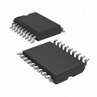
XRT5683AID-F Exar Corporation, XRT5683AID-F Datasheet

XRT5683AID-F
Specifications of XRT5683AID-F
Available stocks
Related parts for XRT5683AID-F
XRT5683AID-F Summary of contents
Page 1
... CC TPOS 17 TCLK 16 TNEG 12 TGND 14 Rev. 2.0.2 2010 EXAR Corporation, 48720 Kato Road, Fremont, CA 94538 TM TTL Compatible Interface Device Can Be Used as a Line Interface Unit With- out Clock Recovery APPLICATIONS T1, T2, E1 & E2 Rates, PCM Line Interface Network Multiplexing and Terminating Equipment attenuated by -10dB cable loss at one-half the bit rate ...
Page 2
XR-T5683A PIN CONFIGURATION PDC 1 18 RXDATA RXDATA BIAS 5 14 TANK BIAS 6 13 RGND 7 12 RCLK Lead PDIP (0.300”) PIN DESCRIPTION Pin # ...
Page 3
ELECTRICAL CHARACTERISTICS Test Conditions 5.0V 5 Parameters DC Electrical Characteristics Supply Voltage Supply Current Receiver Section Tank Drive Current Clock Output Low Clock Output High Data Output Low Data Output High Transmitter Section Driver Output Low ...
Page 4
XR-T5683A ELECTRICAL CHARACTERISTICS (CONT’D) Parameters AC Electrical Characteristics (Cont’d) Transmitter Section Pulse Width at 8.448MHz Output Rise Time Output Fall Time Output Pulse Imbalance Specifications are subject to change without notice Notes Bold face parameters are covered by production test ...
Page 5
Table 1 shows typical expected jitter tolerance. The following measurements have been done at a transmission rate of T1 (1.544MHz). (See Figure 2 ). Jitter 10Hz 100Hz 500Hz 1kHz 2kHz 3kHz 4kHz Table 1. Jitter Tolerance at 1.544Mbps with 6db ...
Page 6
XR-T5683A RXDATA+ RCLK Output at Pin 8 RPOS Output at Pin 11 RNEG Output at Pin 10 Figure 3. Receiver Timing Diagram With 1-1-1-1-1-1 Pattern TCLK Clock to Pin 16 TPOS to Pin 17 TNEG to Pin 12 Bipolar Signal ...
Page 7
Input 8.448MHz Pulse Generator Notes 1 Inputs that are not connected to pulse generator will be tied includes probe and jig capacitance. Input Pulse From Generator 10% Output From Pin 13 or Pin 15 Fall Time ...
Page 8
XR-T5683A 0 TIP RING PE65415 1:1:1 0 0.1 F Rev. 2.0 RXDATA+ 390 TXDATA+ 2 RXDATA- 5 BIAS TXDATA TGND 6 TANK BIAS 0.1 ...
Page 9
INPUT AND OUTPUT TRANSFORMERS Pulse Engineering types PE-65415, PE-65771 or PE-65835 transformers, may be used for both the input and output transformers. These three parts, which are all 1CT:2CT turns ratio and have similar electrical specifications, are wound on small, ...
Page 10
XR-T5683A 18 LEAD PLASTIC DUAL-IN-LINE Seating Plane L B SYMBOL 0.030 Note: The control dimension is the inch column ...
Page 11
LEAD SMALL OUTLINE (300 MIL JEDEC SOIC Seating Plane e SYMBOL Note: The control dimension is the millimeter column Rev. 2.0.2 Rev. 1. ...
Page 12
... While the information in this publication has been carefully checked; no responsibility, however, is assumed for inaccuracies. EXAR Corporation does not recommend the use of any of its products in life support applications where the failure or malfunction of the product can reasonably be expected to cause failure of the life support system or to significantly affect its safety ectiveness. Products are not authorized for use in such applications unless EXAR Corporation receives, in writing, assurances to its satisfaction that: (a) the risk of injury or damage has been minimized ...


