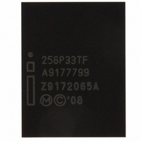
RC28F256P33TFA NUMONYX, RC28F256P33TFA Datasheet - Page 20

RC28F256P33TFA
Manufacturer Part Number
RC28F256P33TFA
Description
IC FLASH 256MBIT 95NS 64EZBGA
Manufacturer
NUMONYX
Series
Axcell™r
Specifications of RC28F256P33TFA
Format - Memory
FLASH
Memory Type
FLASH
Memory Size
256M (16Mx16)
Speed
95ns
Interface
Parallel
Voltage - Supply
2.3 V ~ 3.6 V
Operating Temperature
-40°C ~ 85°C
Package / Case
64-EZBGA
Cell Type
NOR
Density
256Mb
Interface Type
Parallel/Serial
Boot Type
Top
Address Bus
25b
Operating Supply Voltage (typ)
2.5/3/3.3V
Operating Temp Range
-40C to 85C
Package Type
EZBGA
Sync/async
Async/Sync
Operating Temperature Classification
Industrial
Operating Supply Voltage (min)
2.3V
Operating Supply Voltage (max)
3.6V
Word Size
16b
Number Of Words
32M
Supply Current
50mA
Mounting
Surface Mount
Pin Count
64
Lead Free Status / RoHS Status
Contains lead / RoHS non-compliant
Other names
902063
902063
RC28F256P33TF 902063
902063
RC28F256P33TF 902063
Available stocks
Company
Part Number
Manufacturer
Quantity
Price
Company:
Part Number:
RC28F256P33TFA
Manufacturer:
Micron Technology Inc
Quantity:
10 000
Table 7:
Datasheet
20
Notes:
1.
2.
3.
4.
5.
Others
Mode
First command cycle address should be the same as the operation’s target address.
DBA = Device Base Address (NOTE: needed for dual-die 512Mbit device)
DnA = Address within the device.
IA = Identification code address offset.
CFI-A = Read CFI address offset.
WA = Word address of memory location to be written.
BA = Address within the block.
OTP-RA = OTP register address.
LRA = Lock Register address.
RCD = Read Configuration Register data on A[16:1].
ID = Identifier data.
CFI-D = CFI data on DQ[15:0].
SRD = Status Register data.
WD = Word data.
N = Word count of data to be loaded into the write buffer.
OTP-D = OTP register data.
LRD = Lock Register data.
The second cycle of the Buffered Program Command is the word count of the data to be loaded into the write buffer. This
is followed by up to 512 words of data.Then the confirm command (0xD0) is issued, triggering the array programming
operation.
The confirm command (0xD0) is followed by the buffer data.
The second cycle is a Sub-Op-Code, the data written on third cycle is N-1; 1=< N <=512. The subsequent cycles load
data words into the program buffer at a specified address until word count is achieved, after the data words are loaded,
the final cycle is the confirm cycle 0xD0)
Command Bus Cycles (Sheet 2 of 2)
Blank Check
Extended Function
Interface
command
Command
(5)
Cycles
Bus
>2
2
Oper
Write
Write
First Bus Cycle
Addr
WA
BA
(1)
Data
0xBC
0xEB
(2)
Oper
Write
Write
Second Bus Cycle
Order Number: 320003-09
Addr
WA
BA
(1)
P33-65nm
Data
Sub-Op
code
Mar 2010
D0
(2)


