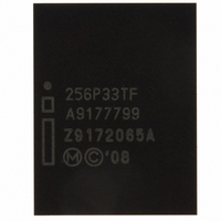
RC28F256P33TFA NUMONYX, RC28F256P33TFA Datasheet - Page 21

RC28F256P33TFA
Manufacturer Part Number
RC28F256P33TFA
Description
IC FLASH 256MBIT 95NS 64EZBGA
Manufacturer
NUMONYX
Series
Axcell™r
Specifications of RC28F256P33TFA
Format - Memory
FLASH
Memory Type
FLASH
Memory Size
256M (16Mx16)
Speed
95ns
Interface
Parallel
Voltage - Supply
2.3 V ~ 3.6 V
Operating Temperature
-40°C ~ 85°C
Package / Case
64-EZBGA
Cell Type
NOR
Density
256Mb
Interface Type
Parallel/Serial
Boot Type
Top
Address Bus
25b
Operating Supply Voltage (typ)
2.5/3/3.3V
Operating Temp Range
-40C to 85C
Package Type
EZBGA
Sync/async
Async/Sync
Operating Temperature Classification
Industrial
Operating Supply Voltage (min)
2.3V
Operating Supply Voltage (max)
3.6V
Word Size
16b
Number Of Words
32M
Supply Current
50mA
Mounting
Surface Mount
Pin Count
64
Lead Free Status / RoHS Status
Contains lead / RoHS non-compliant
Other names
902063
902063
RC28F256P33TF 902063
902063
RC28F256P33TF 902063
Available stocks
Company
Part Number
Manufacturer
Quantity
Price
Company:
Part Number:
RC28F256P33TFA
Manufacturer:
Micron Technology Inc
Quantity:
10 000
P33-65nm
7.0
7.1
Note:
7.2
Datasheet
21
Read Operation
The device can be in any of four read states: Read Array, Read Identifier, Read Status
or Read Query. Upon power-up, or after a reset, the device defaults to Read Array
mode. To change the read state, the appropriate read command must be written to the
device (see
sections describe read-mode operations in detail.
The device supports two read modes: asynchronous page mode and synchronous burst
mode. Asynchronous page mode is the default read mode after device power-up or a
reset. The RCR must be configured to enable synchronous burst reads of the flash
memory array (see
Asynchronous Page-Mode Read
Following a device power-up or reset, asynchronous page mode is the default read
mode and the device is set to Read Array mode. However, to perform array reads after
any other device operation (e.g. write operation), the Read Array command must be
issued in order to read from the flash memory array.
Asynchronous page-mode reads can only be performed when RCR.15 is set
The Clear Status Register command clears the status register. It functions independent
of VPP. The WSM sets and clears SR[7,6,2], but it sets bits SR[5,3,1] without clearing
them. The Status Register should be cleared before starting a command sequence to
avoid any ambiguity. A device reset also clears the Status Register.
To perform an asynchronous page-mode read, an address is driven onto the address
bus, and CE# and ADV# are asserted. WE# and RST# must already have been
deasserted. WAIT is deasserted during asynchronous page mode. ADV# can be driven
high to latch the address, or it must be held low throughout the read cycle. CLK is not
used for asynchronous page-mode reads, and is ignored. If only asynchronous reads
are to be performed, CLK should be tied to a valid V
and ADV# must be tied to ground. Array data is driven onto DQ[15:0] after an initial
access time t
In asynchronous page mode, sixteen data words are “sensed” simultaneously from the
flash memory array and loaded into an internal page buffer. The buffer word
corresponding to the initial address on the Address bus is driven onto DQ[15:0] after
the initial access delay. The lowest four address bits determine which word of the
16-word page is output from the data buffer at any given time.
Synchronous Burst-Mode Read
To perform a synchronous burst-read, an initial address is driven onto the address bus,
and CE# and ADV# are asserted. WE# and RST# must already have been deasserted.
ADV# is asserted, and then deasserted to latch the address. Alternately, ADV# can
remain asserted throughout the burst access, in which case the address is latched on
the next valid CLK edge while ADV# is asserted.
During synchronous array and non-array read modes, the first word is output from the
data buffer on the next valid CLK edge after the initial access latency delay (see
11.1.2, “Latency Count” on page
following a minimum delay. However, for a synchronous non-array read, the same word
of data will be output on successive clock edges until the burst length requirements are
satisfied. Refer to the following waveforms for more detailed information:
•
Figure 20, “Synchronous Single-Word Array or Non-array Read Timing” on page 53
Section 6.2, “Device Command Bus Cycles” on page
AVQV
delay. (see
Section 11.1, “Read Configuration Register” on page
Section 15.0, “AC Characteristics” on page
35). Subsequent data is output on valid CLK edges
IH
level, WAIT signal can be floated
18). The following
Order Number:320003-09
34).
48).
Section
Mar 2010


