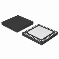
ADP3212MNR2G ON Semiconductor, ADP3212MNR2G Datasheet - Page 15

ADP3212MNR2G
Manufacturer Part Number
ADP3212MNR2G
Description
IC CTLR BUCK 7BIT 2PHASE 48QFN
Manufacturer
ON Semiconductor
Datasheet
1.NCP3218MNR2G.pdf
(35 pages)
Specifications of ADP3212MNR2G
Applications
Controller, Intel IMVP-6.5™
Voltage - Input
3.3 V ~ 22 V
Number Of Outputs
1
Voltage - Output
0.3 V ~ 1.5V
Operating Temperature
-40°C ~ 100°C
Mounting Type
Surface Mount
Package / Case
48-TFQFN Exposed Pad
Output Voltage
0.9512 V
Output Current
52 A
Input Voltage
8 V to 19 V
Supply Current
7 mA
Switching Frequency
300 KHz
Mounting Style
SMD/SMT
Maximum Operating Temperature
+ 100 C
Minimum Operating Temperature
- 40 C
Lead Free Status / RoHS Status
Lead free / RoHS Compliant
Available stocks
Company
Part Number
Manufacturer
Quantity
Price
Company:
Part Number:
ADP3212MNR2G
Manufacturer:
ON Semiconductor
Quantity:
950
Part Number:
ADP3212MNR2G
Manufacturer:
ON/安森美
Quantity:
20 000
Setting Switch Frequency
Master Clock Frequency in PWM Mode
PWM, the clock frequency is set by an external resistor
connected from the RT pin to GND. The frequency is
constant at a given VID code but varies with the VID
voltage: the lower the VID voltage, the lower the clock
frequency. The variation of clock frequency with VID
voltage maintains constant V
power conversion efficiency at lower VID voltages. Figure
VCC
When the APD3212/NCP3218/NCP3218G runs in
I
I
I
RAMP
R
R
R
= A
= A
= A
C
C
C
A
A
A
R
R
R
D
R
R
D
R
D
COMP
x I
x I
x I
RAMP
RAMP
RAMP
−
+
−
+
−
+
Oscillator
Oscillator
Oscillator
R
Clock
Clock
Clock
A
C
0.2 V
FB
0.2 V
0.2 V
C
+
−
A
CORE
FB
+
R
FBRTN
+
−
+
−
C
S
+
−
B
ripple and improves
B
+
Figure 18. 3−Phase PWM Mode Operation
Flip−Flop
+
_
RD
S
Flip−Flop
Flip−Flop
S
RD
S
RD
S
DAC
+
_
LLINE
Q
CSCOMP
Q
Q
http://onsemi.com
Gate Driver
Gate Driver
IN
IN
DRVH
DRVH
DRVL
DRVL
BST
BST
SW
SW
15
+
−
SWFB1
SWFB3
SWFB2
CSREF
C
DRVH2
DRVL2
PWM3
DRVH1
DRVL1
R
7 shows the relationship between clock frequency and VID
voltage, parameterized by RT resistance.
the clock by the number of phases in use.
Switching Frequency in RPM Mode; Single−Phase
Operation
controlled by the ripple voltage on the COMP pin, rather
than by the master clock. Each time the COMP pin voltage
BST2
CS
BST1
CS
SW2
SW1
To determine the switching frequency per phase, divide
In single−phase RPM mode, the switching frequency is
CSSUM
Gate Driver
100 W
100 W
IN
DRVH
DRVL
VCC
VCC
BST
SW
100 W
R
R
R
PH
PH
PH
R
R
L
L
VCC
L
L
R
L
L
LOAD


