LS013B7DH01 Sharp Microelectronics, LS013B7DH01 Datasheet
LS013B7DH01
Specifications of LS013B7DH01


Related parts for LS013B7DH01


LS013B7DH01 Summary of contents
Page 1
... Technical Literature TFT-LCD Module Model No. LS013B7DH01 The technical Literature is subject to change without any prior notice for the purpose of product improvement. Please contact Sharp or its representative before designing your product based on this literature. Liquid Crystal Display Group SHARP CORPORATION No. Date For Notice ...
Page 2
REF.PAGE DATE PARAGRAPH DRAWING No. 1st July 2010 P7 Table3-1 P14 Table6-4 16th Aug 2010 P19 6-5-5 COM Inversion P23 8-1) Outline dimension RECORDS OF REVISION REVISED No. Weight was filled in. (Mass: 3.0g) Power consumption and condition2 typ were ...
Page 3
... Contact and consult with a SHARP sales representative for any questions about this device. SPEC No. LCP-2110019B NOTICE ・Office automation ・Telecommunication equipment ・Industrial control ・Consumer electronics ・Nuclear power control equipment MODEL No. PAGE LS013B7DH01 1 ...
Page 4
... As this LCD module is composed electronic circuits sensitive to electrostatic discharge of 200V or more. Handle with care using cautions for the followings: Operators Operators must wear anti-static wears to prevent electrostatic charge up to and discharge from human body. SPEC No. MODEL No. LCP-2110019B [For handling and system design] PAGE LS013B7DH01 2 ...
Page 5
... Containers and styroform used in transporation and storage may charge electrostatic (from friction and peeling) or electrostatic charge from human body, etc. may cause containers and styroform to have induced charge. Proper electrostatic measure should be taken for containers and storage material. SPEC No. MODEL No. LCP-2110019B LS013B7DH01 PAGE 3 ...
Page 6
... Also, storing the LCD panel in high humidity will damage the polarizer. Store in normal room temperature as much as possible. (3) Keeping Method a. Don't keeping under the direct sunlight. SPEC No. MODEL No. LCP-2110019B [For operating LCD module] [Precautions for Storage] b. Keeping in the tray under the dark place. PAGE LS013B7DH01 4 ...
Page 7
... This liquid crystal panel contains only an extremely small amount of liquid crystal (approximately 100mg) and therefore it will not leak even if the panel should break. Its median lethal dose (LD50) is greater than 2,000 mg/kg and a mutagenetic (Aims test: negative) material is used. SPEC No. MODEL No. LCP-2110019B [Other Notice] Discarding liquid crystal modules PAGE LS013B7DH01 5 ...
Page 8
... Input terminal names and functions...............................................................................................8 5. Absolute Maximum Rating ..............................................................................................................9 6. Electrical characteristics ...............................................................................................................10 7. Optical characteristics...................................................................................................................21 8. Module outline ................................................................................................................................23 9. External capacitors ........................................................................................................................24 10. External Power Supply Circuit ....................................................................................................25 11. Zebra connector ...........................................................................................................................26 12. Packaging......................................................................................................................................27 13. Reliability Test Conditions ..........................................................................................................29 SPEC No. MODEL No. LCP-2110019B LS013B7DH01 Contents PAGE 6 ...
Page 9
... Dot pitch Pixel Array Outline Dimension Mass Surface Hardness (Note) Detail dimension and tolerance are shown in fig. 8-1 SPEC No. MODEL No. LCP-2110019B LS013B7DH01 Specification 3.2 (1.26”) 20.88 (H) × 24.36 (V) 144 (H) × 168 (V) 0.145 (H) × 0.145 (V) Stripe Array 24.88 (W) × 33.00 (H) × 1.64 (D) 3 ...
Page 10
... Display ON/OFF signal Power supply (Analog) Power supply (Digital) COM inversion select terminal GND(Digital) GND(Analog) - Test terminal - Test terminal External COM signal input EXTMODE=”H” MODEL No. PAGE LS013B7DH01 Remark 【Remark4-1】 【Remark4-1】 【Remark4-3】 【Remark4-2】 【Remark4-1】 【Remark4-1】 8 ...
Page 11
... Operating temperature is the temperature that guarantees only for the operation. For contrast, response time, and other display quality determination, use Ta=+25℃. SPEC No. MODEL No. LCP-2110019B Symbol MIN. VDDA -0.3 VDD -0.3 -0.3 Tstg -30 Topr1 -20 PAGE LS013B7DH01 MAX. Unit Remark +5.8 V +5.8 V [Remark5-1] VDD V [Remark5-2] V +80 ℃ [Remark5-3,4] +70 [Remark5-5] ℃ ...
Page 12
... Applies to SCLK, SI, SCS, DISP, EXTCOMIN. SPEC No. LCP-2110019B symbol MIN. TYP. VDDA +4.8 +5.0 VDD +4.8 +5.0 VIH +2.70 +3.00 VIL VSS VSS MODEL No. PAGE LS013B7DH01 VSS(GND)=0V、Ta=+25℃ MAX. Unit Remark +5.5 V +5.5 V [Remark6-1] *VDD V [Remark6-2] VSS+0. ...
Page 13
... Remark 2) When power off, VDD and VDDA are same time or VDDA shoud be faster than the VDD. SPEC No. LCP-2110019B On Sequence Normal operation ③※1 ④※1 ② Normal operation Normal operation Normal operation T4: 30us or more T5 more T6 more MODEL No. LS013B7DH01 Off sequence ⑤ ⑥ ⑦ GND GND GND ※2 GND ※2 GND T3: 30us or more PAGE ...
Page 14
... TYP trSCS - - tfSCS - - twSCSH twSCSL 1 - tsSCS 3 - thSCS 1 - fSI - 0.5 trSI - - tfSI - - tsSI (120) - thSI (125) - trSCLK - - tfSCLK - - twSCLKH 200 450 twSCLKL 200 450 fEXTCOMIN 1 trEXTCOMIN - - twEXTCOMIN - - 1 trDISP - - tfDISP - - MODEL No. PAGE LS013B7DH01 MAX Unit Remark MHz 1000 MAX Unit Remark MHz [Remark6- ...
Page 15
... EXTCOMIN signal 90% 90% EXTCOMIN 10% 10% trEXTCOMIN tfEXTCOMIN DISP signal 90% 90% DISP 10% 10% trDISP tfDISP ※SCS,SI,SCLK、DISP、EXTCOMIN: 3V input voltage SPEC No. LCP-2110019B twSCSH 10% tfSI twSCLKH twSCLKL 90% 50% 50% 50% 10% fEXTCOMIN 50% 50% twEXTCOMINH MODEL No. PAGE LS013B7DH01 twSCSL 90% 50% 50% 10% thSCS tfSCS 50% 50% 13 ...
Page 16
... This is value in steady condition, not the falue of peak power at the time of COM operation. Some marging for power supply is recommended. We recommend capacitor for VDD and VDDA. (If VDD and VDDA are on separate systems, we recommend capacitor for each.) SPEC No. LCP-2110019B MIN TYP MAX - MODEL No. PAGE LS013B7DH01 Ta=25℃ unit Remark uW [Remark6-4] uW [Remark6-4] 14 ...
Page 17
... SCS becomes “L”, M0 and M2 are cleared. SPEC No. LCP-2110019B D141 D142 D143 D144 Data writing period (8ck) (144ck) st latch block of binary driver on panel. st latch is being transferred (written) to pixel internal memory circuit. MODEL No. PAGE LS013B7DH01 thSCS DUMMY DATA(don't care) Data transfer period (16ck) 15 twSCSL ...
Page 18
... AG7 D1 D2 D143 D144 Data writing period (144ck) st latch block of binary driver on panel. st latch to pixel internal memory circuit at the same time. MODEL No. LS013B7DH01 D4 D141 D142 D143 D144 AG0 AG1 DUMMY DATA(don't care) Data transfer period (144ck) (8ck(Dummy)+8ck(Address)=16ck) GL2nd line ...
Page 19
... Refer to 6-5-4) All Clear Mode to execute clear. DUMMY DATA: Dummy data. It can be “H” or “L” (“L” is recommended.) ※ M1: Frame inversion flag is enabled when EXTMODE=”L” ※ When SCS becomes “L”, M0 and M2 are cleared. SPEC No. LCP-2110019B tV thSCS MODEL No. PAGE LS013B7DH01 twSCSL DUMMY DATA(don't care) 17 ...
Page 20
... DUMMY DATA: Dummy data. It can be “H” or “L” (“L” is recommended.) ※ M1: Frame inversion flag is enabled when EXTMODE=”L”. ※ When SCS becomes “L”, M0 and M2 are cleared. SPEC No. LCP-2110019B tV twSCSH twSCSL thSCS M2 DUMMY DATA(don't care) Data transfer period (More than 13ck) MODEL No. PAGE LS013B7DH01 DUMMY DATA(don't care) 18 ...
Page 21
... COM ※3:LC inversion polarity has been set by the rising edge of EXTCOMIN. ※4:The period of EXTCOMIN should be constant. SPEC No. LCP-2110019B ※1 fCOM ※2 ※ 1 ※ 2 fEXTCOMIN ※3 ※4 MODEL No. LS013B7DH01 ※1 ※2 twEXTCOMINH ※ 1 fCOM ※ 2 twEXTCOMINH ※3 fCOM ※4 PAGE 19 ...
Page 22
... P1,L168 Gate line address setting GL AG0 AG1 AG2 AG3 AG4 AG5 AG6 AG7 : : : : 161 162 163 164 165 166 167 168 SPEC No. LCP-2110019B UP P144,L1 Display Display side up side up P144,L168 : : : : : MODEL No. PAGE LS013B7DH01 20 ...
Page 23
... T (0.3) τr 10 τ (0.307) y (0.330) Measurement equipment (LCD-5200) Light source Light receiver Light source LCD panel MODEL No. PAGE LS013B7DH01 MAX. unit Remark °(degree) [Remark7-1] °(degree) °(degree) [Remark7-2、3] % [Remark7- [Remark 7-3,4] ms [Remark7-3] Normal line Light receiver -30° ...
Page 24
... It’s difined by the time change of optical receiver output when signal is input to display white or black White SPEC No. LCP-2110019B Normal Line Δθ22 Δθ11 6 o’clock direction Reflection intensity in white display Reflection intensity in black display Black Time MODEL No. LS013B7DH01 Δθ12 Δθ21 White PAGE 22 ...
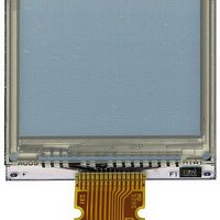
Page 25
... Module outline 8-1) Outline dimension of the 1.26” (144 x 168) panel fig.8-1 SPEC No. MODEL No. LCP-2110019B LS013B7DH01 fig. 8-3 PAGE 23 fig. 8-2 ...
Page 26
... C3:VDD- VSS: rank B For actual use, please evaluate their conformity with your system and design. (Capacitor pressure resistance can be larger than resistance indicated above.) SPEC No. LCP-2110019B 0.1uF Ceramic capacitor 1uF Ceramic capacitor ※Above circuit and parts are only recommendation. MODEL No. PAGE LS013B7DH01 24 ...
Page 27
... The reference circuit is shown below. SPEC No. MODEL No. LCP-2110019B Model Number S-8821 LM2750 Vin [V] min max min 2.8 5.0 4.9 2.7 5.6 4.8 S-8821 LM2750 PAGE LS013B7DH01 Note Charge pump type Charge pump type Vout Iout [A] typ max 5.0 5.1 0.04 5.0 5.2 0.04 25 ...
Page 28
... Contact Resistance :lower than 100Ω 【Recommended zebra connector】 Shin-Etsu Polymer: SX type Recommended size L:27.7±0.2mm W:1.5±0.1mm H:2.0±0.1mm P:0.03mm Recommended compression ratio:15±8% The zebra connector placement position 1.SX Specifications(A figure of reference) SPEC No. MODEL No. LCP-2110019B LS013B7DH01 Fig 11-1 PAGE 26 ...
Page 29
... There should be no condensation at low temperature and high humidity. No harmful gas, such as acid or alkali, which causes severe corrosion on electronic parts and wiring, are to be detected. About 3 months be made over 50%RH and take effective measure such as use of earth when opening the package. MODEL No. PAGE LS013B7DH01 27 ...
Page 30
... Packaging SPEC No. MODEL No. LCP-2110019B LS013B7DH01 Packageing size :578mmx382mmx153mm Fig. 12-2 Packaging Form PAGE 28 ...
Page 31
... Ta=-30degrees Celsius (1h)~+80 degrees Celsius (1h cycle ±200V、200pF(0Ω) each terminai: 1 time :LCD panel with polarizer :Center of LCD panel :φ10mm column :1mm/minute :fixed on stage :5 seconds after achivement of the press strength,then reless it. MODEL No. PAGE LS013B7DH01 Remark 240h 240h 240h 240h 240h 29 ...