EVAL-ADF7012DBZ5 Analog Devices Inc, EVAL-ADF7012DBZ5 Datasheet - Page 21
EVAL-ADF7012DBZ5
Manufacturer Part Number
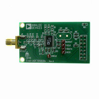
EVAL-ADF7012DBZ5
Description
BOARD DAUGHTER FOR ADF7012
Manufacturer
Analog Devices Inc
Type
Transmitterr
Datasheet
1.EVAL-ADF7012EB1.pdf
(28 pages)
Specifications of EVAL-ADF7012DBZ5
For Use With/related Products
ADF7012
Lead Free Status / RoHS Status
Lead free / RoHS Compliant


433 MHz OPERATION
The recommendations here are guidelines only. The design
should be subject to internal testing prior to ETSI site testing.
Matching components need to be adjusted for board layout.
The ETSI standard EN 300-220 governs operation in the
433.050 MHz to 434.790 MHz band. For many systems, 10%
duty is sufficient for the transmitter to output 10 dBm.
Design Criteria
433.92 MHz center frequency
FSK modulation
10 mW output power
200 m range
Meets ETSI 300-220
The main requirement in the design of this remote is a long
battery life and sufficient range. It is possible to adjust the
output power of the ADF7012 to increase the range depending
on the antenna performance.
The center frequency is 433.92 MHz. It is possible to operate the
VCO at this frequency. Figure 36 shows the inductor value vs.
center frequency. The inductor chosen is 22 nH. Coilcraft
inductors such as 0603-CS-22NXJBU are recommended.
Crystal and PFD
The phase noise requirement is such to ensure the power at
the edge of the band is < −36 dBm. The PFD is chosen to
minimize spurious levels (beat note and reference), and to
ensure a quick crystal power-up time.
PFD = 4.9152 MHz − Power-Up Time 1.6 ms. Figure 10 shows a
typical power-up time for a 4 MHz crystal.
N-Divider
The N Divider is determined as being:
Deviation
The deviation is set to ± 50 kHz to accommodate a simple
receiver architecture.
The modulation steps available are in 4.9152 MHz/2
Nint = 88
Nfrac = (1152)/4096
VCO divide-by-2 is not enabled
Modulation steps = 300 Hz
Modulation number = 50 kHz/300Hz = 167
14
:
Rev. A | Page 21 of 28
Bias Current
Because low current is desired, a 2.0 mA VCO bias can be used.
Additional bias current reduces any spurious, but increases
current consumption.
The PA bias can be set to 5.5 mA and achieve 10 dBm.
Loop Filter Bandwidth
The loop filter is designed with ADIsimSRD Design Studio.
The loop bandwidth design requires that the channel power
be < −36 dBm at ±870 kHz from the center. A loop bandwidth
of close to 160 kHz strikes a good balance between lock time for
data rates, including 32 kbps and spurious suppression. If it is
found that pulling of the VCO is more than desired in OOK
mode, the bandwidth could be increased.
Design of Harmonic Filter
The main requirement of the harmonic filter should ensure
that the third harmonic level is < −30 dBm. A fifth-order
Chebyshev filter is recommended to achieve this, and a
suggested starting point is given next. The Pi format is chosen
to minimize the more expensive inductors.
Component Values—Crystal: 4.9152 MHz
Loop Filter
Icp
LBW
C1
C2
C3
R1
R2
Matching
L1
L2
C14
Harmonic Filter
L4
L5
C15
C16
C17
2.0 mA
100 kHz
680 pF
12 nF
270 pF
910 Ω
3.3 kΩ
22 nH
10 pF
470 pF
22 nH
22 nH
3.3 pF
8.2 pF
3.3 pF
ADF7012
Related parts for EVAL-ADF7012DBZ5
Image
Part Number
Description
Manufacturer
Datasheet
Request
R

Part Number:
Description:
IC, ADJ LDO REG, 1.5V TO 5V 250mA MSOP-8
Manufacturer:
Vishay
Datasheet:

Part Number:
Description:
IC, ADJ LDO REG, 1.5V TO 5V 0.6A 8-TSSOP
Manufacturer:
Vishay
Datasheet:
Part Number:
Description:
IC, ADJ LDO REG, 1.5V TO 5V 250mA MSOP-8
Manufacturer:
Vishay
Datasheet:

Part Number:
Description:
IC ADJ LDO REG 1.5V TO 5V 150mA 5-SOT-23
Manufacturer:
Vishay
Datasheet:

Part Number:
Description:
BOARD EVAL AS1324-AD
Manufacturer:
austriamicrosystems
Datasheet:
Part Number:
Description:
IC, ADJ LDO REG, 1.5V TO 5V 0.6A 8-TSSOP
Manufacturer:
Vishay
Datasheet:

Part Number:
Description:
IC, ADJ LDO REG, 1.5V TO 5V, 0.3A, MSOP8
Manufacturer:
Vishay
Datasheet:
Part Number:
Description:
IC, ADJ LDO REG, 1.5V TO 5V, 0.3A, MSOP8
Manufacturer:
Vishay
Datasheet:
Part Number:
Description:
IC, ADJ LDO REG 1.215V TO 5V 0.3A MSOP-8
Manufacturer:
Vishay
Datasheet:
Part Number:
Description:
IC, ADJ LDO REG 1.215V TO 5V 0.3A MSOP-8
Manufacturer:
Vishay
Datasheet:

Part Number:
Description:
±1.7g Dual-Axis IMEMS Accelerometer Evaluation Board
Manufacturer:
Analog Devices Inc
Datasheet:

Part Number:
Description:
IC MULTIPLIER ANALOG 8-SOIC T/R
Manufacturer:
Analog Devices Inc
Datasheet:

Part Number:
Description:
IC ANALOG MULTIPLIER 8-DIP
Manufacturer:
Analog Devices Inc
Datasheet:
Part Number:
Description:
IC ANALOG MULTIPLIER 8-SOIC
Manufacturer:
Analog Devices Inc
Datasheet:
Part Number:
Description:
IC ANALOG MULTIPLIER 8-DIP
Manufacturer:
Analog Devices Inc
Datasheet: