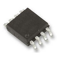
MCP3550-50-E/SN Microchip Technology, MCP3550-50-E/SN Datasheet - Page 12

MCP3550-50-E/SN
Manufacturer Part Number
MCP3550-50-E/SN
Description
IC, ADC, 22BIT, 12.5SPS, SOIC-8
Manufacturer
Microchip Technology
Datasheet
1.MCP3550-50-ESN.pdf
(30 pages)
Specifications of MCP3550-50-E/SN
Resolution (bits)
22bit
Sampling Rate
12.5SPS
Input Channel Type
Differential
Data Interface
3-Wire, Serial
Supply Voltage Range - Analog
2.7V To 5.5V
Supply Current
120µA
Lead Free Status / RoHS Status
Lead free / RoHS Compliant
MCP3550/1/3
4.0
The MCP3550/1/3 devices are 22-bit delta-sigma
ADCs that include fully differential analog inputs, a
third-order delta-sigma modulator, a fourth-order
modified SINC decimation filter, an on-chip, low-noise
internal oscillator, a power supply monitoring circuit and
an SPI 3-wire digital interface. These devices can be
easily used to measure low-frequency, low-level
signals such as those found in pressure transducers,
temperature, strain gauge, industrial control or process
control applications. The power supply range for this
product family is 2.7V to 5.5V; the temperature range is
-40°C to +125°C. The functional block diagram for the
MCP3550/1/3 devices is shown in Figure 4-1.
A Power-On Reset (POR) monitoring circuit is included
to ensure proper power supply voltages during the
conversion process. The clock source for the part is
internally generated to ±0.5% over the full-power
supply voltage range and industrial temperature range.
This stable clock source allows for superior conversion
repeatability and minimal drift across conversions.
The MCP3550/1/3 devices employ a delta-sigma
conversion technique to realize up to 22 bits of no
missing code performance with 21.9 Effective Number
of Bits (ENOB). These devices provide single-cycle
conversions with no digital filter settling time. Every
conversion includes an internal offset and gain auto-
calibration to reduce device error. These calibrations
are transparent to the user and are done in real-time
during the conversion. Therefore, these devices do not
require any additional time or conversion to proceed,
allowing easy usage of the devices for multiplexed
applications. The MCP3550/1/3 devices incorporate a
fourth-order digital decimation filter in order to allow
superior averaging performance, as well as excellent
line frequency rejection capabilities. The oversampling
frequency also reduces any external anti-aliasing filter
requirements.
FIGURE 4-1:
DS21950C-page 12
Analog Input
Differential
DEVICE OVERVIEW
Calibration
Gain and
Offset
MCP3550/1/3 Functional Block Diagram.
Transfer
Charge
Third-Order
Modulator
Oscillator
Internal
Reference
Clock
Input
Stream
Bit
The MCP3550/1/3 devices communicate with a simple
3-wire SPI interface. The interface controls the
conversion start event, with an added feature of an
auto-conversion at system power-up by tying the CS
pin to logic-low. The device can communicate with bus
speeds of up to 5 MHz, with 50 pF capacitive loading.
The interface offers two conversion modes: Single
Conversion mode for multiplexed applications and a
Continuous Conversion mode for multiple conversions
in series. Every conversion is independent of each
other. That is, all internal registers are flushed between
conversions. When the device is not converting, it auto-
matically goes into Shutdown mode and, while in this
mode, consumes less than 1 µA.
Filter (SINC
Decimation
Digital
4
)
Conversion
Code
© 2005 Microchip Technology Inc.
SPI 3-wire
Interface
Output
Code


