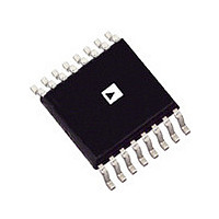
ADM3491ARUZ-1 Analog Devices Inc, ADM3491ARUZ-1 Datasheet - Page 4

ADM3491ARUZ-1
Manufacturer Part Number
ADM3491ARUZ-1
Description
IC RS422/RS485 TXRX 250KBPS 3.6V SOIC-14
Manufacturer
Analog Devices Inc
Type
Transceiverr
Datasheet
1.ADM3491ARUZ-1.pdf
(20 pages)
Specifications of ADM3491ARUZ-1
Device Type
Differential Line Transceiver
Ic Interface Type
RS422, RS485
No. Of Drivers
1
Supply Voltage Range
3V To 3.6V
Msl
MSL 1 - Unlimited
No. Of Driver/receivers
1/1
Number Of Drivers/receivers
1/1
Protocol
RS422, RS485
Voltage - Supply
3 V ~ 3.6 V
Mounting Type
Surface Mount
Package / Case
16-TSSOP
Data Rate
10Mbps
Number Of Receivers
1
Number Of Transmitters
1
Number Of Transceivers
1
Data Transmission Topology
Multidrop/Multipoint
Receiver Signal Type
Differential
Transmitter Signal Type
Differential
Single Supply Voltage (typ)
3.3V
Single Supply Voltage (min)
3V
Single Supply Voltage (max)
3.6V
Dual Supply Voltage (typ)
Not RequiredV
Dual Supply Voltage (min)
Not RequiredV
Dual Supply Voltage (max)
Not RequiredV
Supply Current
2.2mA
Power Supply Requirement
Single
Operating Temp Range
-40C to 85C
Operating Temperature Classification
Industrial
Mounting
Surface Mount
Pin Count
16
Package Type
TSSOP
Transceiver Type
RS485
No. Of Channels
1
Rohs Compliant
Yes
Data Rate Max
30Mbps
Lead Free Status / RoHS Status
Lead free / RoHS Compliant
Lead Free Status / RoHS Status
Lead free / RoHS Compliant, Lead free / RoHS Compliant
Other names
ADM3491ARUZ
ADM3491ARUZ
ADM3491ARUZ
ADM3483/ADM3485/ADM3488/ADM3490/ADM3491
SPECIFICATIONS
V
Table 2.
Parameter
DRIVER
DRIVER INPUT LOGIC
RECEIVER
POWER SUPPLY CURRENT
1
∆V
CC
Differential Output Voltage (V
Δ |V
Common-Mode Output Voltage (V
Δ |V
CMOS Input Logic Threshold Low (V
CMOS Input Logic Threshold High (V
CMOS Logic Input Current (I
Input Current—A, B (I
Output Leakage—Y, Z (I
Output Leakage (Y, Z) in Shutdown Mode (I
Differential Input Threshold Voltage (V
Input Hysteresis (Δ V
CMOS Output Voltage High (V
CMOS Output Voltage Low (V
Three-State Output Leakage Current (I
Input Resistance (R
Supply Current (I
Supply Current in Shutdown Mode (I
Driver Short-Circuit Output Current (I
Receiver Short-Circuit Output Current (I
OD
= 3.3 V ± 0.3 V, T
and ∆V
OD
OC
| for Common-Mode Output Voltage
| for Complementary Output States
OC
are the changes in V
CC
)
IN
A
)
TH
= T
IN2
)
)
O
)
MIN
OD
IN1
to T
OL
OD
and V
)
OH
)
)
)
MAX
OC
OC
, unless otherwise noted.
IL
, respectively, when DI input changes state.
)
IH
SHDN
)
OSD
)
TH
OZR
OSR
)
)
)
)
1
)
1
O
)
Min
2.0
1.5
1.5
2.0
−0.2
V
12
±8
CC
– 0.4
Rev. D | Page 4 of 20
Typ
0.1
−0.1
0.01
−0.01
50
1.1
0.95
0.002
Max
0.2
3
0.2
0.8
±2
1.0
−0.8
+0.2
0.4
±1
2.2
1.9
1
−250
250
±60
Unit
V
V
V
V
V
V
V
V
μA
mA
mA
μA
μA
μA
μA
V
mV
V
V
μA
kΩ
mA
mA
μA
mA
mA
mA
Test Conditions/Comments
R
R
R
R
R
R
DE, DI, RE
DE, DI, RE
DE, DI, RE
V
V
V
ADM3491 only
V
ADM3491 only
V
ADM3491 only
V
ADM3491 only
−7 V < V
V
I
I
V
−7 V < V
DE = V
DE = 0 V, RE = 0 V, no load, DI = 0 V or V
DE = 0 V, RE = V
V
V
0 V < V
OUT
OUT
L
L
L
L
L
L
IN
IN
IN
IN
IN
IN
CM
CC
OUT
OUT
= 54 Ω or 100 Ω (see Figure 7)
= 100 Ω (RS-422), V
= 54 Ω (RS-485) (see Figure 7)
= 60 Ω (RS-485), V
= 54 Ω or 100 Ω (see Figure 7)
= 54 Ω or 100 Ω (see Figure 7)
= 12 V, DE = 0 V, V
= −7 V, DE = 0 V, V
= 12 V, DE = 0 V, RE = 0 V, V
= −7 V, DE = 0 V, RE = 0 V, V
= 12 V, DE = 0 V, RE = V
= −7 V, DE = 0 V, RE = V
= 3.6 V, 0 V ≤ V
= −1.5 mA, V
= 2.5 mA, V
= 0 V
= −7 V
= 12 V
CC
RO
CM
CM
, RE = 0 V or V
< V
< +12 V
< +12 V
CC
ID
CC
ID
= 200 mV (see Figure 9)
, DI = V
OUT
= 200 mV (see Figure 9)
CC
CC
CC
≤ V
CC
CC
= 3.3 V (see Figure 8)
= 0 V or 3.6 V
= 0 V or 3.6 V
, no load, DI = 0 V or V
= 3.3 V ± 5% (see Figure 7)
CC
CC
CC
CC
or 0 V
, V
, V
CC
CC
CC
CC
= 0 V or 3.6 V,
= 0 V or 3.6 V,
= 0 V or 3.6 V,
= 0 V or 3.6 V,
CC
CC


