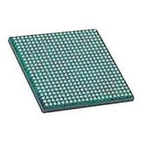
LFXP2-40E-5FN672C LATTICE SEMICONDUCTOR, LFXP2-40E-5FN672C Datasheet - Page 5

LFXP2-40E-5FN672C
Manufacturer Part Number
LFXP2-40E-5FN672C
Description
IC, LATTICEXP2 FPGA, 435MHZ, FPBGA-672
Manufacturer
LATTICE SEMICONDUCTOR
Series
LatticeXP2r
Datasheet
1.LFXP2-5E-5TN144C.pdf
(93 pages)
Specifications of LFXP2-40E-5FN672C
No. Of Logic Blocks
40000
No. Of Macrocells
20000
Family Type
LatticeXP2
No. Of Speed Grades
5
No. Of I/o's
540
Clock Management
PLL
Total Ram Bits
885Kbit
Lead Free Status / RoHS Status
Lead free / RoHS Compliant
- Current page: 5 of 93
- Download datasheet (2Mb)
Lattice Semiconductor
Figure 2-1. Simplified Block Diagram, LatticeXP2-17 Device (Top Level)
PFU Blocks
The core of the LatticeXP2 device is made up of logic blocks in two forms, PFUs and PFFs. PFUs can be pro-
grammed to perform logic, arithmetic, distributed RAM and distributed ROM functions. PFF blocks can be pro-
grammed to perform logic, arithmetic and ROM functions. Except where necessary, the remainder of this data
sheet will use the term PFU to refer to both PFU and PFF blocks.
Each PFU block consists of four interconnected slices, numbered Slice 0 through Slice 3, as shown in Figure 2-2.
All the interconnections to and from PFU blocks are from routing. There are 50 inputs and 23 outputs associated
with each PFU block.
Programmable
Function Units
(PFUs)
sysMEM Block
RAM
DSP Blocks
SPI Port
On-chip
Oscillator
sysCLOCK PLLs
2-2
Flexible Routing
sysIO Buffers,
Pre-Engineered Source
Synchronous Support
LatticeXP2 Family Data Sheet
Architecture
JTAG Port
Flash
Related parts for LFXP2-40E-5FN672C
Image
Part Number
Description
Manufacturer
Datasheet
Request
R

Part Number:
Description:
IC, LATTICEXP2 FPGA, 435MHZ, FPBGA-484
Manufacturer:
LATTICE SEMICONDUCTOR
Datasheet:
Part Number:
Description:
ISPLSI2032-80LT44Lattice Semiconductor [In-System Programmable High Density PLD]
Manufacturer:
Lattice Semiconductor Corp.
Datasheet:
Part Number:
Description:
IC PROGRAMMED LATTICE GAL 16V8
Manufacturer:
Lattice Semiconductor Corp.
Datasheet:
Part Number:
Description:
357-036-542-201 CARDEDGE 36POS DL .156 BLK LOPRO
Manufacturer:
Lattice Semiconductor Corp.
Datasheet:
Part Number:
Description:
357-036-542-201 CARDEDGE 36POS DL .156 BLK LOPRO
Manufacturer:
Lattice Semiconductor Corp.
Datasheet:
Part Number:
Description:
357-036-542-201 CARDEDGE 36POS DL .156 BLK LOPRO
Manufacturer:
Lattice Semiconductor Corp.
Datasheet:
Part Number:
Description:
357-036-542-201 CARDEDGE 36POS DL .156 BLK LOPRO
Manufacturer:
Lattice Semiconductor Corp.
Datasheet:
Part Number:
Description:
357-036-542-201 CARDEDGE 36POS DL .156 BLK LOPRO
Manufacturer:
Lattice Semiconductor Corp.
Datasheet:
Part Number:
Description:
357-036-542-201 CARDEDGE 36POS DL .156 BLK LOPRO
Manufacturer:
Lattice Semiconductor Corp.
Datasheet:
Part Number:
Description:
357-036-542-201 CARDEDGE 36POS DL .156 BLK LOPRO
Manufacturer:
Lattice Semiconductor Corp.
Datasheet:
Part Number:
Description:
357-036-542-201 CARDEDGE 36POS DL .156 BLK LOPRO
Manufacturer:
Lattice Semiconductor Corp.
Datasheet:
Part Number:
Description:
357-036-542-201 CARDEDGE 36POS DL .156 BLK LOPRO
Manufacturer:
Lattice Semiconductor Corp.
Datasheet:
Part Number:
Description:
357-036-542-201 CARDEDGE 36POS DL .156 BLK LOPRO
Manufacturer:
Lattice Semiconductor Corp.
Datasheet:
Part Number:
Description:
In-system programmable 3.3V generic digital switch
Manufacturer:
Lattice Semiconductor Corp.
Datasheet:
Part Number:
Description:
High performance E2CMOS PLD generic array logic, 15ns, quarter power
Manufacturer:
Lattice Semiconductor Corp.
Datasheet:


