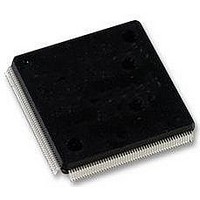
LFXP6C-5QN208C LATTICE SEMICONDUCTOR, LFXP6C-5QN208C Datasheet - Page 6

LFXP6C-5QN208C
Manufacturer Part Number
LFXP6C-5QN208C
Description
FPGA, 1.8V FLASH, INSTANT ON, SMD
Manufacturer
LATTICE SEMICONDUCTOR
Series
LatticeXPr
Datasheet
1.LFXP3C-3QN208C.pdf
(130 pages)
Specifications of LFXP6C-5QN208C
No. Of Logic Blocks
720
No. Of Macrocells
3000
Family Type
LatticeXP
No. Of Speed Grades
5
No. Of I/o's
142
Clock Management
PLL
Core Supply Voltage Range
1.71V To 3.465V
Lead Free Status / RoHS Status
Lead free / RoHS Compliant
Available stocks
Company
Part Number
Manufacturer
Quantity
Price
Company:
Part Number:
LFXP6C-5QN208C
Manufacturer:
Lattice Semiconductor Corporation
Quantity:
10 000
- Current page: 6 of 130
- Download datasheet (2Mb)
Lattice Semiconductor
Slice
Each slice contains two LUT4 lookup tables feeding two registers (programmed to be in FF or Latch mode), and
some associated logic that allows the LUTs to be combined to perform functions such as LUT5, LUT6, LUT7 and
LUT8. There is control logic to perform set/reset functions (programmable as synchronous/asynchronous), clock
select, chip-select and wider RAM/ROM functions. Figure 2-3 shows an overview of the internal logic of the slice.
The registers in the slice can be configured for positive/negative and edge/level clocks.
There are 14 input signals: 13 signals from routing and one from the carry-chain (from adjacent slice or PFU).
There are 7 outputs: 6 to routing and one to carry-chain (to adjacent PFU). Table 2-1 lists the signals associated
with each slice.
Figure 2-3. Slice Diagram
Control Signals
selected and
inverted per
slice in routing
From
Routing
Note: Some interslice signals
are not shown.
CLK
LSR
M1
M0
CE
C1
D1
C0
D0
A1
B1
A0
B0
Different slice / PFU Fast Carry Out (FCO)
Different slice / PFU Fast Carry In (FCI)
To / From
To / From
LUT4 &
CARRY
LUT4 &
CARRY
CO
CO
CI
CI
2-3
SUM
SUM
F
F
OFX0
Expansion
LUT
Mux
Slice
LatticeXP Family Data Sheet
D
D
Latch
Latch
FF/
FF/
OFX1
F1
OFX0
F0
Q0
Q1
To
Routing
Architecture
Related parts for LFXP6C-5QN208C
Image
Part Number
Description
Manufacturer
Datasheet
Request
R

Part Number:
Description:
FPGA, 1.8V FLASH, INSTANT ON, SMD
Manufacturer:
LATTICE SEMICONDUCTOR
Datasheet:

Part Number:
Description:
IC FPGA 5.8KLUTS 188I/O 256-BGA
Manufacturer:
Lattice
Datasheet:

Part Number:
Description:
FPGA - Field Programmable Gate Array 5.8K LUTS 142 I/O
Manufacturer:
Lattice
Datasheet:

Part Number:
Description:
FPGA - Field Programmable Gate Array 5.8K LUTs 100 IO 1.8 /2.5/3.3V -4 Spd I
Manufacturer:
Lattice
Datasheet:

Part Number:
Description:
FPGA - Field Programmable Gate Array 5.8K LUTs 142 IO 1.8 /2.5/3.3V -4 Spd
Manufacturer:
Lattice
Datasheet:

Part Number:
Description:
FPGA - Field Programmable Gate Array 5.8K LUTs 188 I/O 1.8/2.5/3.3V -4 Spd
Manufacturer:
Lattice
Datasheet:
Part Number:
Description:
FPGA LatticeXP Family 6000 Cells 360MHz 130nm (CMOS) Technology 1.8V/2.5V/3.3V 256-Pin FBGA Tray
Manufacturer:
LATTICE SEMICONDUCTOR
Datasheet:
Part Number:
Description:
FPGA LatticeXP Family 6000 Cells 400MHz 130nm (CMOS) Technology 1.8V/2.5V/3.3V 256-Pin FBGA Tray
Manufacturer:
LATTICE SEMICONDUCTOR
Datasheet:

Part Number:
Description:
FPGA LatticeXP Family 6000 Cells 360MHz 130nm (CMOS) Technology 1.8V/2.5V/3.3V 208-Pin PQFP Tray
Manufacturer:
Lattice
Datasheet:

Part Number:
Description:
IC FPGA 5.8KLUTS 100I/O 144-TQFP
Manufacturer:
Lattice
Datasheet:

Part Number:
Description:
IC FPGA 5.8KLUTS 100I/O 144-TQFP
Manufacturer:
Lattice
Datasheet:

Part Number:
Description:
IC FPGA 5.8KLUTS 100I/O 144-TQFP
Manufacturer:
Lattice
Datasheet:

Part Number:
Description:
IC FPGA 5.8KLUTS 100I/O 144-TQFP
Manufacturer:
Lattice
Datasheet:


