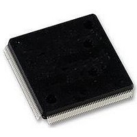
LFXP6C-5QN208C LATTICE SEMICONDUCTOR, LFXP6C-5QN208C Datasheet - Page 9

LFXP6C-5QN208C
Manufacturer Part Number
LFXP6C-5QN208C
Description
FPGA, 1.8V FLASH, INSTANT ON, SMD
Manufacturer
LATTICE SEMICONDUCTOR
Series
LatticeXPr
Datasheet
1.LFXP3C-3QN208C.pdf
(130 pages)
Specifications of LFXP6C-5QN208C
No. Of Logic Blocks
720
No. Of Macrocells
3000
Family Type
LatticeXP
No. Of Speed Grades
5
No. Of I/o's
142
Clock Management
PLL
Core Supply Voltage Range
1.71V To 3.465V
Lead Free Status / RoHS Status
Lead free / RoHS Compliant
Available stocks
Company
Part Number
Manufacturer
Quantity
Price
Company:
Part Number:
LFXP6C-5QN208C
Manufacturer:
Lattice Semiconductor Corporation
Quantity:
10 000
- Current page: 9 of 130
- Download datasheet (2Mb)
Lattice Semiconductor
Table 2-4. PFU Modes of Operation
Routing
There are many resources provided in the LatticeXP devices to route signals individually or as buses with related
control signals. The routing resources consist of switching circuitry, buffers and metal interconnect (routing) seg-
ments.
The inter-PFU connections are made with x1 (spans two PFU), x2 (spans three PFU) and x6 (spans seven PFU).
The x1 and x2 connections provide fast and efficient connections in horizontal, vertical and diagonal directions. The
x2 and x6 resources are buffered allowing both short and long connections routing between PFUs.
The ispLEVER design tool takes the output of the synthesis tool and places and routes the design. Generally, the
place and route tool is completely automatic, although an interactive routing editor is available to optimize the
design.
Clock Distribution Network
The clock inputs are selected from external I/O, the sysCLOCK™ PLLs or routing. These clock inputs are fed
through the chip via a clock distribution system.
Primary Clock Sources
LatticeXP devices derive clocks from three primary sources: PLL outputs, dedicated clock inputs and routing. Lat-
ticeXP devices have two to four sysCLOCK PLLs, located on the left and right sides of the device. There are four
dedicated clock inputs, one on each side of the device. Figure 2-5 shows the 20 primary clock sources.
1. These modes are not available in PFF blocks
MUX 16x1 x 1
MUX 2x1 x 8
MUX 4x1 x 4
MUX 8x1 x 2
LUT 6x 2 or
LUT 4x8 or
LUT 5x4 or
LUT 7x1 or
Logic
2-bit Counter x 4
2-bit Comp x 4
2-bit Add x 4
2-bit Sub x 4
Ripple
2-6
DPR16x2 x 2
DPR16x4 x 1
SPR16x2 x 4
SPR16x4 x 2
SPR16x8 x 1
RAM
1
LatticeXP Family Data Sheet
ROM16x1 x 8
ROM16x2 x 4
ROM16x4 x 2
ROM16x8 x 1
ROM
Architecture
Related parts for LFXP6C-5QN208C
Image
Part Number
Description
Manufacturer
Datasheet
Request
R

Part Number:
Description:
FPGA, 1.8V FLASH, INSTANT ON, SMD
Manufacturer:
LATTICE SEMICONDUCTOR
Datasheet:

Part Number:
Description:
IC FPGA 5.8KLUTS 188I/O 256-BGA
Manufacturer:
Lattice
Datasheet:

Part Number:
Description:
FPGA - Field Programmable Gate Array 5.8K LUTS 142 I/O
Manufacturer:
Lattice
Datasheet:

Part Number:
Description:
FPGA - Field Programmable Gate Array 5.8K LUTs 100 IO 1.8 /2.5/3.3V -4 Spd I
Manufacturer:
Lattice
Datasheet:

Part Number:
Description:
FPGA - Field Programmable Gate Array 5.8K LUTs 142 IO 1.8 /2.5/3.3V -4 Spd
Manufacturer:
Lattice
Datasheet:

Part Number:
Description:
FPGA - Field Programmable Gate Array 5.8K LUTs 188 I/O 1.8/2.5/3.3V -4 Spd
Manufacturer:
Lattice
Datasheet:
Part Number:
Description:
FPGA LatticeXP Family 6000 Cells 360MHz 130nm (CMOS) Technology 1.8V/2.5V/3.3V 256-Pin FBGA Tray
Manufacturer:
LATTICE SEMICONDUCTOR
Datasheet:
Part Number:
Description:
FPGA LatticeXP Family 6000 Cells 400MHz 130nm (CMOS) Technology 1.8V/2.5V/3.3V 256-Pin FBGA Tray
Manufacturer:
LATTICE SEMICONDUCTOR
Datasheet:

Part Number:
Description:
FPGA LatticeXP Family 6000 Cells 360MHz 130nm (CMOS) Technology 1.8V/2.5V/3.3V 208-Pin PQFP Tray
Manufacturer:
Lattice
Datasheet:

Part Number:
Description:
IC FPGA 5.8KLUTS 100I/O 144-TQFP
Manufacturer:
Lattice
Datasheet:

Part Number:
Description:
IC FPGA 5.8KLUTS 100I/O 144-TQFP
Manufacturer:
Lattice
Datasheet:

Part Number:
Description:
IC FPGA 5.8KLUTS 100I/O 144-TQFP
Manufacturer:
Lattice
Datasheet:

Part Number:
Description:
IC FPGA 5.8KLUTS 100I/O 144-TQFP
Manufacturer:
Lattice
Datasheet:


