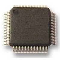
UPD78F0886GA(A)-GAM-AX NEC, UPD78F0886GA(A)-GAM-AX Datasheet - Page 88

UPD78F0886GA(A)-GAM-AX
Manufacturer Part Number
UPD78F0886GA(A)-GAM-AX
Description
8BIT MCU, 60K FLASH, 3KB RAM, CAN
Manufacturer
NEC
Datasheet
1.UPD78F0886GAA-GAM-AX.pdf
(129 pages)
Specifications of UPD78F0886GA(A)-GAM-AX
Controller Family/series
UPD78F
No. Of I/o's
41
Ram Memory Size
3KB
Cpu Speed
20MHz
No. Of Timers
8
No. Of Pwm Channels
6
Digital Ic Case Style
LQFP
Core Size
8bit
Program Memory Size
60KB
Lead Free Status / RoHS Status
Lead free / RoHS Compliant
- Current page: 88 of 129
- Download datasheet (645Kb)
88
[Instruction format]
[Operation]
[Operand]
[Flag]
[Description]
[Description example]
flag.
OR1
• The logical sum of bit data of the destination operand (dst) specified by the 1st operand and the source
• The operation result is stored in the CY flag (because of the destination operand (dst)).
OR1 CY, P2.5; The logical sum of port 2 bit 5 and the CY flag is obtained and the result is stored in the CY
operand (src) specified by the 2nd operand is obtained and the result is stored in the destination operand
(dst).
Mnemonic
Z
OR1
AC
CY, saddr.bit
CY, sfr.bit
CY, A.bit
CY, PSW.bit
CY, [HL].bit
OR1 dst, src
dst ← dst ∨ src
CY
×
Operand(dst,src)
CHAPTER 5 EXPLANATION OF INSTRUCTIONS
User's Manual U12326EJ4V0UM
1 Bit Data Logical Sum
Or Single Bit
Related parts for UPD78F0886GA(A)-GAM-AX
Image
Part Number
Description
Manufacturer
Datasheet
Request
R

Part Number:
Description:
16/8 bit single-chip microcomputer
Manufacturer:
NEC
Datasheet:

Part Number:
Description:
Dual audio power amp circuit
Manufacturer:
NEC
Datasheet:

Part Number:
Description:
Dual comparator
Manufacturer:
NEC
Datasheet:

Part Number:
Description:
MOS type composite field effect transistor
Manufacturer:
NEC
Datasheet:

Part Number:
Description:
50 V/100 mA FET array incorporating 2 N-ch MOSFETs
Manufacturer:
NEC
Datasheet:

Part Number:
Description:
6-pin small MM high-frequency double transistor
Manufacturer:
NEC
Datasheet:

Part Number:
Description:
6-pin small MM high-frequency double transistor
Manufacturer:
NEC
Datasheet:

Part Number:
Description:
6-pin small MM high-frequency double transistor
Manufacturer:
NEC
Datasheet:

Part Number:
Description:
6-pin small MM high-frequency double transistor
Manufacturer:
NEC
Datasheet:

Part Number:
Description:
Twin transistors equipped with different model chips(6P small MM)
Manufacturer:
NEC
Datasheet:

Part Number:
Description:
Bipolar analog integrated circuit
Manufacturer:
NEC
Datasheet:


