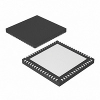
PIC24FJ192GA106-I/MR Microchip Technology, PIC24FJ192GA106-I/MR Datasheet - Page 8

PIC24FJ192GA106-I/MR
Manufacturer Part Number
PIC24FJ192GA106-I/MR
Description
IC, 16BIT MCU, PIC24F, 32MHZ, QFN-64
Manufacturer
Microchip Technology
Series
PIC® 24Fr
Datasheets
1.PIC24FJ128GA008-IPT.pdf
(12 pages)
2.PIC24FJ128GA106-IPT.pdf
(14 pages)
3.PIC24FJ128GA106-IPT.pdf
(330 pages)
4.PIC24FJ128GA106-IPT.pdf
(52 pages)
5.PIC24FJ128GB110-IPF.pdf
(292 pages)
Specifications of PIC24FJ192GA106-I/MR
Controller Family/series
PIC24
No. Of I/o's
53
Ram Memory Size
16KB
Cpu Speed
32MHz
No. Of Timers
5
Core Size
16 Bit
Program Memory Size
192KB
Peripherals
ADC, Comparator, PWM, RTC, Timer
Core Processor
PIC
Speed
32MHz
Connectivity
I²C, PMP, SPI, UART/USART
Number Of I /o
53
Program Memory Type
FLASH
Ram Size
16K x 8
Voltage - Supply (vcc/vdd)
2 V ~ 3.6 V
Data Converters
A/D 16x10b
Oscillator Type
Internal
Operating Temperature
-40°C ~ 85°C
Package / Case
64-VFQFN, Exposed Pad
Processor Series
PIC24FJ
Core
PIC
Data Bus Width
16 bit
Data Ram Size
16 KB
Interface Type
I2C, SPI, UART
Maximum Clock Frequency
32 MHz
Number Of Programmable I/os
53
Number Of Timers
5
Maximum Operating Temperature
+ 85 C
Mounting Style
SMD/SMT
3rd Party Development Tools
52713-733, 52714-737, 53276-922, EWDSPIC
Development Tools By Supplier
PG164130, DV164035, DV244005, DV164005, PG164120, DM240011, DM240001
Minimum Operating Temperature
- 40 C
On-chip Adc
10 bit, 16 Channel
Lead Free Status / RoHS Status
Lead free / RoHS Compliant
For Use With
876-1004 - PIC24 BREAKOUT BOARD
Eeprom Size
-
Lead Free Status / Rohs Status
Details
PIC24FJ256GA110 FAMILY
22. Module: Core (Code Protection)
23. Module: SPI/PPS
DS80368J-page 8
When General Segment Code Protection has
been enabled (GCP Configuration bit is pro-
grammed), applications are unable to write to the
first 512 bytes of the program memory space
(0000h through 0200h). In applications that may
require the interrupt vectors to be changed during
run time, such as bootloaders, modifications to the
interrupt vector tables will not be possible.
Work around
Create two new interrupt vector tables, one each
for the IVT and AIVT, in an area of program space
beyond the affected region. Map the addresses in
the old vector tables to the new tables. These new
tables can then be modified as needed to the
actual addresses of the ISRs.
Affected Silicon Revisions
The ALTRP/ASCK1 functionality is not supported
by the A3 revision of this part family.
Work around
None.
Affected Silicon Revisions
A3
A3
X
X
A5
A5
24. Module: Oscillator (LPRC)
25. Module: CTMU (A/D Trigger)
The LPRC may not automatically restart following
BOR events (i.e., when supply voltage sags to
between the BOR and POR thresholds, then
returns to above the BOR level). When this hap-
pens, systems that use the LPRC clock may not
work. This includes the PLL, Two-Speed Start-up,
Fail-Safe Clock Monitor and the WDT.
Work around
For PLL issues: Select a non-PLL Clock mode as
the initial start-up mode, using the FNOSC Config-
uration bits (CW2<10:8>). After the application has
initialized, switch to a PLL Clock mode in software
using the NOSC bits (OSCCON<10:8>). Allow
10 microseconds to elapse between application
start-up and a software clock switch.
For WDT issues: Disable the WDT by programming
the FWDTEN bit (CW1<7>). After the application
has initialized, enable the WDT in software by
setting the SWDTEN bit (RCON<5>). Allow
10 microseconds to elapse between application
start-up and setting SWDTEN.
Affected Silicon Revisions
The CTMU may not trigger an automatic A/D con-
version after the current source is turned off. This
happens even when the A/D trigger control bit,
CTTRIG (CTMUCON<8>), has been set.
Work around
Perform a manual A/D conversion by clearing the
SAMP bit (AD1CON1<1>) immediately after the
CTMU current source has been stopped.
Affected Silicon Revisions
A3
A3
X
X
A5
A5
2010 Microchip Technology Inc.


