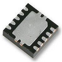
LT3970EDDB-3.3#PBF Linear Technology, LT3970EDDB-3.3#PBF Datasheet - Page 15

LT3970EDDB-3.3#PBF
Manufacturer Part Number
LT3970EDDB-3.3#PBF
Description
IC, STEP-DOWN REGULATOR, DFN-10
Manufacturer
Linear Technology
Datasheet
1.LT3970EMS-3.3PBF.pdf
(22 pages)
Specifications of LT3970EDDB-3.3#PBF
Primary Input Voltage
12V
No. Of Outputs
1
Output Voltage
3.3V
Output Current
350mA
No. Of Pins
10
Operating Temperature Range
-40°C To +125°C
Peak Reflow Compatible (260 C)
Yes
Msl
MSL 1 - Unlimited
Rohs Compliant
Yes
Lead Free Status / RoHS Status
Lead free / RoHS Compliant
Available stocks
Company
Part Number
Manufacturer
Quantity
Price
APPLICATIONS INFORMATION
Be aware that while V
may rise up to several hundred μA and the part may begin
to switch while the internal circuitry starts up. Figure 7
shows the startup behavior of a typical application with
different programmed V
Shorted and Reversed Input Protection
If the inductor is chosen so that it won’t saturate excessively,
a LT3970 buck regulator will tolerate a shorted output.
There is another situation to consider in systems where
the output will be held high when the input to the LT3970
is absent. This may occur in battery charging applications
or in battery backup systems where a battery or some
other supply is diode ORed with the LT3970’s output. If
the V
(either by a logic signal or because it is tied to V
the LT3970’s internal circuitry will pull its quiescent current
through its SW pin. This is fi ne if the system can tolerate
a few μA in this state. If the EN pin is grounded, the SW
pin current will drop to 0.7μA. However, if the V
grounded while the output is held high, regardless of EN,
parasitic diodes inside the LT3970 can pull current from
the output through the SW pin and the V
shows a circuit that will run only when the input voltage
is present and that protects against a shorted or reversed
input.
IN
pin is allowed to fl oat and the EN pin is held high
V
IN
R3
R4
Figure 6. Enable
IN
V
EN
IN(EN)
IN
is below 4.2V, the input current
1V
.
LT3970
+
–
SHDN
3970 F06
IN
pin. Figure 8
IN
IN
), then
pin is
Figure 7. V
No-Load Current, and V
Figure 8. Diode D4 Prevents a Shorted Input from Discharging a
Backup Battery Tied to the Output. It Also Protects the Circuit from
a Reversed Input. The LT3970 Runs Only when the Input is Present
LT3970/LT3970-3.3/LT3970-5
V
IN
160
120
160
120
MBRS140
80
40
80
40
IN
0
4
3
2
1
0
0
4
3
2
1
0
D4
0
0
Start-Up of Front Page Application with V
1
2
V
EN
GND
IN
2
IN(EN)
LT3970
4
BD
INPUT VOLTAGE (V)
INPUT VOLTAGE (V)
3
BOOST
6
programmed as in Figure 6.
FB
SW
4
8
5
10
6
V
R3 = 11M
R4 = 1M
V
R3 = 5M
R4 = 1M
IN(EN)
IN(EN)
12
7
3970 F08
= 12V
= 6V
3970 F07
+
14
8
V
BACKUP
OUT
OUT
15
= 3.3V,
3970fa


