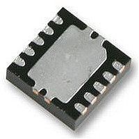
LT3970EDDB-3.3#PBF Linear Technology, LT3970EDDB-3.3#PBF Datasheet - Page 8

LT3970EDDB-3.3#PBF
Manufacturer Part Number
LT3970EDDB-3.3#PBF
Description
IC, STEP-DOWN REGULATOR, DFN-10
Manufacturer
Linear Technology
Datasheet
1.LT3970EMS-3.3PBF.pdf
(22 pages)
Specifications of LT3970EDDB-3.3#PBF
Primary Input Voltage
12V
No. Of Outputs
1
Output Voltage
3.3V
Output Current
350mA
No. Of Pins
10
Operating Temperature Range
-40°C To +125°C
Peak Reflow Compatible (260 C)
Yes
Msl
MSL 1 - Unlimited
Rohs Compliant
Yes
Lead Free Status / RoHS Status
Lead free / RoHS Compliant
Available stocks
Company
Part Number
Manufacturer
Quantity
Price
PIN FUNCTIONS
LT3970/LT3970-3.3/LT3970-5
FB (Pin 1, LT3970 Only): The LT3970 Regulates the FB
Pin to 1.21V. Connect the feedback resistor divider tap to
this pin.
V
3.3 and LT3970-5 regulate the V
respectively. This pin connects to the internal feedback
divider that programs the fi xed output voltage.
EN (Pin 2): The part is in shutdown when this pin is low
and active when this pin is high. The hysteretic threshold
voltage is 1V going up and 0.97V going down. Tie to V
if shutdown feature is not used. The EN threshold is ac-
curate only when V
4.2V, ground EN to place the part in shutdown.
V
internal circuitry and to the internal power switch. This
pin must be locally bypassed.
BLOCK DIAGRAM
8
V
IN
OUT
IN
C1
(Pin 3): The V
(Pin 1, LT3970-3.3 and LT3970-5 Only): The LT3970-
R
T
10
3
2
9
*LT3970-3.3: R1 = 12.65M, R2 = 7.35M
LT3970-5: R1 = 15.15M, R2 = 4.85M
V
EN
RT
PG
IN
1V
+
–
IN
(4, 5)
GND
IN
pin supplies current to the LT3970’s
is above 4.2V. If V
+
–
INTERNAL 1.21V REF
SHDN
1.09V
R2
1
FB
OUT
LT3970 ONLY
+
–
ERROR
R1
AMP
Pin to 3.3V and 5V
IN
is lower than
LT3970-3.3
LT3970-5
ONLY*
V
R2
C
200kHz TO 2.2MHz
–
+
SLOPE COMP
OSCILLATOR
Burst Mode
DETECT
R1
IN
1
V
OUT
GND (Pins 4, 5, Exposed Pad (Pin 11, DFN Only)): Ground.
Must be soldered to PCB.
SW (Pin 6): The SW pin is the output of an internal power
switch. Connect this pin to the inductor.
BOOST (Pin 7): This pin is used to provide a drive volt-
age, higher than the input voltage, to the internal bipolar
NPN power switch.
BD (Pin 8): This pin connects to the anode of the boost
diode. This pin also supplies current to the LT3970’s internal
regulator when BD is above 3.2V.
PG (Pin 9): The PG pin is the open-drain output of an
internal comparator. PG remains low until the FB pin is
within 10% of the fi nal regulation voltage. PG is valid when
V
RT (Pin 10): A resistor is tied between RT and ground to
set the switching frequency.
IN
is above 4.2V and EN is high.
SWITCH LATCH
R
S
Q
D
BOOST
D
CATCH
BOOST
SW
BD
8
7
6
C3
L1
C2
3990 BD
3970fa
V
OUT


