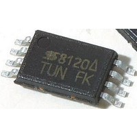
SI9181DQ-AD-T1-E3 Vishay, SI9181DQ-AD-T1-E3 Datasheet - Page 4

SI9181DQ-AD-T1-E3
Manufacturer Part Number
SI9181DQ-AD-T1-E3
Description
IC, ADJ LDO REG, 1.5V TO 5V 0.6A 8-TSSOP
Manufacturer
Vishay
Datasheet
1.SI9181DQ-15-T1-E3.pdf
(11 pages)
Specifications of SI9181DQ-AD-T1-E3
Primary Input Voltage
6V
Output Voltage Adjustable Range
1.5V To 5V
Dropout Voltage Vdo
150mV
No. Of Pins
8
Output Current
600mA
Operating Temperature Range
-40°C To +85°C
Number Of Outputs
1
Polarity
Positive
Input Voltage Max
6 V
Output Voltage
1.5 V to 5 V
Output Type
Adjustable
Dropout Voltage (max)
0.25 V at 200 mA
Line Regulation
0.18 % / V
Load Regulation
30 mV
Maximum Power Dissipation
0.833 W
Maximum Operating Temperature
+ 85 C
Mounting Style
SMD/SMT
Package / Case
TSSOP-8
Minimum Operating Temperature
- 40 C
Lead Free Status / RoHS Status
Lead free / RoHS Compliant
www.vishay.com
4
Si9181
Vishay Siliconix
TIMING WAVEFORMS
PIN CONFIGURATION
PIN DESCRIPTION
Pin Number
1
2
3
4
5
6
7
8
SENSE or ADJ
Name
ERROR
C
DELAY
V
GND
NOISE
V
SD
OUT
IN
Noise bypass pin. For low noise applications, a 0.01-mF or larger ceramic capacitor should be connected from this pin
to ground.
Capacitor connected from this pin to ground will allow a delayed power-on-reset signal at the ERROR (Pin 7) output.
Refer to Figure 4.
Ground pin. Local ground for C
Input supply pin. Bypass this pin with a 2.2-mF ceramic or tantalum capacitor to ground.
Output voltage. Connect C
For fixed output voltage versions, this pin should be connected to V
this voltage feedback pin sets the output voltage via an external resistor divider.
This open drain output is an error flag output which goes low when V
also provides a power-on-reset signal if a capacitor is connected to the DELAY pin.
By applying less than 0.4 V to this pin, the device will be turned off. Connect this pin to V
C
DELAY
NOISE
GND
V
IN
FIGURE 4. Timing Diagram for Power-Up
ERROR
1
2
3
4
0.95 V
V
V
OUT
OUT
V
IN
NOM
TSSOP-8
OUT
Top View
between this pin and ground.
NOISE
t
t
ON
DELAY
and C
OUT
.
8
7
6
5
Function
SD
ERROR
SENSE or ADJ
V
OUT
V
NOM
OUT
OUT
(Pin 5). For adjustable output voltage version,
drops 5% below its nominal voltage. This pin
IN
if unused.
S-50955—Rev. F, 16-May-05
Document Number: 71119


