AD630AD Analog Devices Inc, AD630AD Datasheet - Page 6
AD630AD
Manufacturer Part Number
AD630AD
Description
MODULATOR / DEMODULATOR IC
Manufacturer
Analog Devices Inc
Datasheet
1.AD630JNZ.pdf
(12 pages)
Specifications of AD630AD
Rf Type
Balanced
Supply Voltage Range
± 5V To �� 16.5V
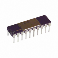
Rf Ic Case Style
DIP
No. Of Pins
20
Operating Temperature Range
-25°C To +85°C
Peak Reflow Compatible (260 C)
No
Leaded Process Compatible
No
Rohs Status
RoHS non-compliant
Function
Modulator/Demodulator
Frequency
2MHz
Package / Case
20-CDIP (0.300", 7.62mm)
Mounting Type
Through Hole
Rohs Compliant
No
Lead Free Status / RoHS Status
Contains lead / RoHS non-compliant
Available stocks
Company
Part Number
Manufacturer
Quantity
Price

Part Number:
AD630AD
Manufacturer:
ADI/亚德诺
Quantity:
20 000


AD630
TWO WAYS TO LOOK AT THE AD630
The functional block diagram of the AD630 (see page 1) shows
the pin connections of the internal functions. An alternative archi-
tectural diagram is shown in Figure 1. In this diagram, the
individual A and B channel preamps, the switch, and the inte-
grator output amplifier are combined in a single op amp. This
amplifier has two differential input channels, only one of which
is active at a time.
HOW THE AD630 WORKS
The basic mode of operation of the AD630 may be easier to recog-
nize as two fixed gain stages which can be inserted into the signal
path under the control of a sensitive voltage comparator. When
the circuit is switched between inverting and noninverting gain, it
provides the basic modulation/demodulation function. The AD630
is unique in that it includes laser wafer trimmed thin-film feed-
back resistors on the monolithic chip. The configuration shown in
Figure 2 yields a gain of ± 2 and can be easily changed to ± 1 by
shifting R
The comparator selects one of the two input stages to complete
an operational feedback connection around the AD630. The
deselected input is off and has a negligible effect on the operation.
When Channel B is selected, the resistors R
connected for inverting feedback as shown in the inverting
gain configuration diagram in Figure 3. The amplifier has suffi-
cient loop gain to minimize the loading effect of R
virtual ground produced by the feedback connection. When the
sign of the comparator input is reversed, Input B will be dese-
lected and A will be selected. The new equivalent circuit will be
the noninverting gain configuration shown in Figure 4. In this
case, R
the amplifier drives this difference voltage to zero, the closed-loop
gain is unaffected.
A
will appear across the op amp input terminals, but since
B
SEL B
SEL A
from its ground connection to the output.
Figure 1. Architectural Block Diagram
Figure 2. AD630 Symmetric Gain ( ± 2)
V
i
10
16
20
19
18
17
1
2
9
16
2.5k
2.5k
R
5k
A
10k
R
5k
A
14
R
B
15
15
10
20
19
18
9
2
A
B
A
B
+V
11
S
–V
8
S
R
10k
10k
F
R
13
R
10k
A
B
F
and R
13
12
14
V
7
O
B/A
B
F
at the
are
–6–
The two closed-loop gain magnitudes will be equal when R
= 1 + R
(R
The 5 kΩ and the two 10 kΩ resistors on the AD630 chip can
be used to make a gain of 2 as shown below. By paralleling
the 10 kΩ resistors to make R
the circuit can be programmed for a gain of ± 1 (as shown in
Figure 9a). These and other configurations using the on-chip
resistors present the inverting inputs with a 2.5 kΩ source imped-
ance. The more complete AD630 diagrams show 2.5 kΩ resistors
available at the noninverting inputs which can be conveniently
used to minimize errors resulting from input bias currents.
CIRCUIT DESCRIPTION
The simplified schematic of the AD630 is shown in Figure 5.
It has been subdivided into three major sections, the comparator,
the two input stages, and the output integrator. The compara-
tor consists of a front end made up of Q52 and Q53, a flip-flop
load formed by Q3 and Q4, and two current steering switching
cells Q28, Q29 and Q30, Q31. This structure is designed so that
a differential input voltage greater than 1.5 mV in magnitude
applied to the comparator inputs will completely select one of
the switching cells. The sign of this input voltage determines
which of the two switching cells is selected.
+V
–V
SEL B
SEL A
S
S
F
+ R
10
11
9
8
Q3
Q52
B
F
Figure 4. Noninverting Gain Configuration
/R
) the parallel equivalent resistance of R
V
i
V
Figure 3. Inverting Gain Configuration
B
Figure 5. AD630 Simplified Schematic
i
, which will result from making R
Q53
CH A–
i
55
Q4
20
10k
5k
5k
R
OFF ADJ
R
R
A
10k
DIFF
A
B
Q62
Q28
i
R
3
22
Q33
B
Q29
Q30
R
Q34
OFF ADJ
CH A+
F
Q65
DIFF
F
i
10k
23
10k
4
equal to 5 kΩ and omitting R
R
2
Q31
F
CH B+
19
Q24
Q67
OFF ADJ
Q35
CM
5
V
O
V
Q36
=
O
Q70
A
(
Q25
= –
1+
OFF ADJ
C122
equal to R
F
C121
CM
R
R
i
and R
R
R
CH B–
73
6
18
F
B
F
A
)
V
Q32
V
i
i
B
Q44
Q74
.
REV. E
COMP
F
13
12
R
F
V
/R
B
B
OUT
/
,
A
Related parts for AD630AD
Image
Part Number
Description
Manufacturer
Datasheet
Request
R

Part Number:
Description:
±1.7g Dual-Axis IMEMS Accelerometer Evaluation Board
Manufacturer:
Analog Devices Inc
Datasheet:

Part Number:
Description:
Inertial Sensor Evaluation System
Manufacturer:
Analog Devices Inc
Datasheet:
Part Number:
Description:
Manufacturer:
Analog Devices Inc
Datasheet:
Part Number:
Description:
Manufacturer:
Analog Devices Inc
Datasheet:
Part Number:
Description:
Manufacturer:
Analog Devices Inc
Datasheet:
Part Number:
Description:
Manufacturer:
Analog Devices Inc
Datasheet:
Part Number:
Description:
Manufacturer:
Analog Devices Inc
Datasheet:
Part Number:
Description:
Manufacturer:
Analog Devices Inc
Datasheet:
Part Number:
Description:
Manufacturer:
Analog Devices Inc
Datasheet:
Part Number:
Description:
Manufacturer:
Analog Devices Inc
Datasheet:
Part Number:
Description:
Manufacturer:
Analog Devices Inc
Datasheet:
Part Number:
Description:
Manufacturer:
Analog Devices Inc
Datasheet:
Part Number:
Description:
Manufacturer:
Analog Devices Inc
Datasheet: