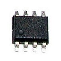
MB85RC128PNF-G-JNE1 Fujitsu, MB85RC128PNF-G-JNE1 Datasheet - Page 5

MB85RC128PNF-G-JNE1
Manufacturer Part Number
MB85RC128PNF-G-JNE1
Description
IC, MEMORY, FRAM, 128K, 12C, 8SOP
Manufacturer
Fujitsu
Datasheet
1.MB85RC128PNF-G-JNE1.pdf
(20 pages)
Specifications of MB85RC128PNF-G-JNE1
Memory Size
128Kbit
Access Time
900ns
Supply Voltage Range
2.7V To 3.6V
Memory Case Style
SOP
No. Of Pins
8
Operating Temperature Range
-40°C To +85°C
Interface
I2C, Serial, 2 Wire
Memory
RoHS Compliant
Memory Configuration
16K X 8
Nvram Features
I2C Bus Specification Version 2.1 Compliant, Fully Controllable By SCL And SDA Ports
Interface Type
I2C, Serial, 2-Wire
Rohs Compliant
Yes
DS05-13110-1E
■ ACKNOWLEDGE (ACK)
• Acknowledge timing overview diagram
In the I
signal indicates that every each 8 bits of the data is successfully sent and received. The information receiver
side usually outputs “L” every time on the 9th SCL clock after each 8 bits are successfully transmitted. On the
transmitter side, the bus is temporarily released to Hi-Z every time on this 9th clock to allow the acknowledge
signal to be received and checked. During this Hi-Z-released period, the receiver side pulls the SDA line down
to indicate “L” that the previous 8bits communication is successfully received.
If the information receiver side detects Stop condition before driving the acknowledge “L”, the read operation
ends and the I
acknowledge “L”, the bus remains in the released state “H” without doing anything.
SCL
SDA
2
C bus, serial data including address or memory information is sent in units of 8 bits. The acknowledge
Start
2
C bus enters the standby state. If Stop condition is not sent, nor does the transmitter detect the
The transmitter side should always release SDA on the
9th bit. At this time, the receiver side outputs a pull-down
to indicate a successful byte transfer (ACK response).
1
2
3
8
MB85RC128
ACK
9
5


