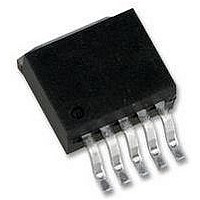
LM2575S-ADJ National Semiconductor, LM2575S-ADJ Datasheet - Page 20

LM2575S-ADJ
Manufacturer Part Number
LM2575S-ADJ
Description
DC/DC Converter IC
Manufacturer
National Semiconductor
Datasheet
1.LM2575S-ADJ.pdf
(28 pages)
Specifications of LM2575S-ADJ
Input Voltage
40V
Output Voltage
37V
No. Of Pins
5
Termination Type
SMD
Mounting Type
Through Hole
Output Current Max
1A
Peak Reflow Compatible (260 C)
No
Supply Voltage Max
40V
Lead Free Status / RoHS Status
Contains lead / RoHS non-compliant
Available stocks
Company
Part Number
Manufacturer
Quantity
Price
Company:
Part Number:
LM2575S-ADJ
Manufacturer:
NS
Quantity:
5 510
Part Number:
LM2575S-ADJ
Manufacturer:
NS/国半
Quantity:
20 000
www.national.com
tance numbers as low as 40°C/W for the SO package, and
30°C/W for the N package can be realized with a carefully
engineered pc board.
Included on the Switchers Made Simple design software is
a more precise (non-linear) thermal model that can be used
to determine junction temperature with different input-output
parameters or different component values. It can also calcu-
late the heat sink thermal resistance required to maintain the
regulators junction temperature below the maximum operat-
ing temperature.
Additional Applications
INVERTING REGULATOR
Figure 10 shows a LM2575-12 in a buck-boost configuration
to generate a negative 12V output from a positive input volt-
age. This circuit bootstraps the regulator's ground pin to the
negative output voltage, then by grounding the feedback pin,
the regulator senses the inverted output voltage and regu-
lates it to −12V.
For an input voltage of 12V or more, the maximum available
output current in this configuration is approximately 0.35A. At
lighter loads, the minimum input voltage required drops to
approximately 4.7V.
The switch currents in this buck-boost configuration are high-
er than in the standard buck-mode design, thus lowering the
available output current. Also, the start-up input current of the
buck-boost converter is higher than the standard buck-mode
regulator, and this may overload an input power source with
a current limit less than 1.5A. Using a delayed turn-on or an
undervoltage lockout circuit (described in the next section)
FIGURE 10. Inverting Buck-Boost Develops −12V
20
would allow the input voltage to rise to a high enough level
before the switcher would be allowed to turn on.
Because of the structural differences between the buck and
the buck-boost regulator topologies, the buck regulator de-
sign procedure section can not be used to select the inductor
or the output capacitor. The recommended range of inductor
values for the buck-boost design is between 68 μH and 220
μH, and the output capacitor values must be larger than what
is normally required for buck designs. Low input voltages or
high output currents require a large value output capacitor (in
the thousands of micro Farads).
The peak inductor current, which is the same as the peak
switch current, can be calculated from the following formula:
Where f
rent operating conditions, the minimum V
worst case. Select an inductor that is rated for the peak cur-
rent anticipated.
Also, the maximum voltage appearing across the regulator is
the absolute sum of the input and output voltage. For a −12V
output, the maximum input voltage for the LM2575 is +28V,
or +48V for the LM2575HV.
The Switchers Made Simple (version 3.3) design software
can be used to determine the feasibility of regulator designs
using different topologies, different input-output parameters,
different components, etc.
osc
= 52 kHz. Under normal continuous inductor cur-
1147515
IN
represents the


