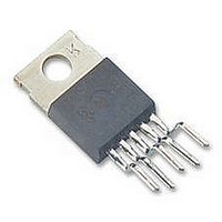
LM2595T-ADJ National Semiconductor, LM2595T-ADJ Datasheet - Page 24

LM2595T-ADJ
Manufacturer Part Number
LM2595T-ADJ
Description
DC/DC Converter IC
Manufacturer
National Semiconductor
Datasheet
1.LM2595T-ADJ.pdf
(29 pages)
Specifications of LM2595T-ADJ
Input Voltage
40V
Output Current
1A
Output Voltage
37V
No. Of Pins
5
Termination Type
Through Hole
Mounting Type
Through Hole
Voltage Regulator Type
Buck Switching
Output Current Max
1A
Lead Free Status / RoHS Status
Contains lead / RoHS non-compliant
Available stocks
Company
Part Number
Manufacturer
Quantity
Price
Part Number:
LM2595T-ADJ
Manufacturer:
NS/国半
Quantity:
20 000
Company:
Part Number:
LM2595T-ADJ/NOPB
Manufacturer:
NS
Quantity:
8 784
www.national.com
Application Information
This circuit has hysteresis
C
120 µF/50V Elec. Panasonic HFQ
C
120 µF/25V Elec. Panasonic HFQ
Because of differences in the operation of the inverting regu-
lator, the standard design procedure is not used to select the
inductor value. In the majority of designs, a 68 µH, 1.5A in-
ductor is the best choice. Capacitor selection can also be
narrowed down to just a few values. Using the values shown
in Figure 25 will provide good results in the majority of invert-
ing designs.
IN
OUT
FIGURE 26. Inverting Regulator Typical Load Current
Regulator starts switching at V
Regulator stops switching at V
:
:
— 220 µF/25V Tant. Sprague 595D
— 22 µF/20V Tant. Sprague 595D
FIGURE 24. Undervoltage Lockout with Hysteresis for Inverting Regulator
IN
IN
= 8V
= 13V
FIGURE 25. Inverting −5V Regulator with Delayed Startup
(Continued)
DS012565-41
24
This type of inverting regulator can require relatively large
amounts of input current when starting up, even with light
loads. Input currents as high as the LM2595 current limit (ap-
prox 1.5A) are needed for at least 2 ms or more, until the out-
put reaches its nominal output voltage. The actual time de-
pends on the output voltage and the size of the output
capacitor. Input power sources that are current limited or
sources that can not deliver these currents without getting
loaded down, may not work correctly. Because of the rela-
tively high startup currents required by the inverting topology,
the delayed startup feature (C1, R
25 is recommended. By delaying the regulator startup, the
input capacitor is allowed to charge up to a higher voltage
before the switcher begins operating. A portion of the high in-
put current needed for startup is now supplied by the input
capacitor (C
pacitor can be made much larger than normal.
INVERTING REGULATOR SHUTDOWN METHODS
To use the ON /OFF pin in a standard buck configuration is
simple, pull it below 1.3V (
turn regulator ON, pull it above 1.3V to shut the regulator
OFF. With the inverting configuration, some level shifting is
required, because the ground pin of the regulator is no
longer at ground, but is now setting at the negative output
voltage level. Two different shutdown methods for inverting
regulators are shown in Figure 27 and Figure 28 .
IN
). For severe start up conditions, the input ca-
DS012565-39
@
25˚C, referenced to ground) to
1
and R
DS012565-40
2
) shown in Figure


