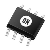
UC3845BD1R2G ON Semiconductor, UC3845BD1R2G Datasheet - Page 14

UC3845BD1R2G
Manufacturer Part Number
UC3845BD1R2G
Description
IC,SMPS CONTROLLER,CURRENT-MODE,BIPOLAR,SOP,8PIN,PLASTIC
Manufacturer
ON Semiconductor
Datasheet
1.UC3844BNG.pdf
(19 pages)
Specifications of UC3845BD1R2G
Rohs Compliant
YES
Number Of Outputs
1
Duty Cycle (max)
48 %
Output Voltage
4.9 V to 5.1 V
Output Current
1000 mA
Mounting Style
SMD/SMT
Package / Case
SOIC-8
Switching Frequency
500 KHz
Operating Supply Voltage
30 V
Maximum Operating Temperature
+ 70 C
Fall Time
50 ns
Minimum Operating Temperature
0 C
Rise Time
50 ns
Synchronous Pin
No
Topology
Boost, Flyback
Lead Free Status / Rohs Status
Lead free / RoHS Compliant
Available stocks
Company
Part Number
Manufacturer
Quantity
Price
Part Number:
UC3845BD1R2G
Manufacturer:
ON/安森美
Quantity:
20 000
1.0nF
1.0nF
10k
10k
The capacitor's equivalent series resistance must limit the Drive Output current to 1.0 A. An additional series resistor
may be required when using tantalum or other low ESR capacitors. The converter's output can provide excellent line
and load regulation by connecting the R2/R1 resistor divider as shown.
The capacitor's equivalent series resistance must limit the Drive Output current to 1.0 A.
An additional series resistor may be required when using tantalum or other low ESR capacitors.
8(14)
8(14)
4(7)
2(3)
1(1)
4(7)
2(3)
1(1)
2.5V
2.5V
Amplifier
Amplifier
Error
Error
R
R
R
R
+
+
Osc
Osc
Internal
0.5mA
Internal
0.5mA
Bias
Bias
Figure 32. Voltage−Inverting Charge Pump Converter
2R
2R
R
R
3.6V
Figure 31. Step−Up Charge Pump Converter
3.6V
UC3845B
UC3845B
5(9)
5(9)
1.0V
1.0V
-
+
-
+
Current Sense
Current Sense
Reference
Comparator
Regulator
Reference
Comparator
Regulator
UVLO
UVLO
V
V
ref
ref
S
R
S
R
http://onsemi.com
T
T
Q
Q
UVLO
V
UVLO
V
CC
CC
PWM
Latch
PWM
Latch
+
-
+
-
14
7(12)
7(12)
34V
34V
V
7(11)
6(10)
7(11)
6(10)
5(8)
3(5)
in
V
5(8)
3(5)
in
= 15V
V
= 15V
O
= 2.5
15
15
+
+
Connect to
Pin 2 for
closed loop
operation.
R2
R1
1N5819
10
10
47
47
) 1
+
1N5819
1N5819
Output Load Regulation
I
O
(Open Loop Configuration)
Output Load Regulation
(mA)
18
32
1N5819
R2
R1
0
2
9
I
O
(mA)
18
36
0
2
9
+
+
47
47
V
−14.4
−13.2
−12.5
−10.6
−11.7
V
V
O
O
O
≈
V
(V)
≈
29.9
28.8
28.3
27.4
24.4
2 (V
O
-V
(V)
in
in
)


