2N6766 International Rectifier, 2N6766 Datasheet - Page 2
2N6766
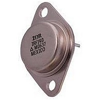
Manufacturer Part Number
2N6766
Description
N CH MOSFET, 200V, 30A, TO-204AE
Manufacturer
International Rectifier
Datasheet
1.IRF250.pdf
(7 pages)
Specifications of 2N6766
Transistor Polarity
N Channel
Continuous Drain Current Id
30A
Drain Source Voltage Vds
200V
On Resistance Rds(on)
85mohm
Rds(on) Test Voltage Vgs
10V
Threshold Voltage Vgs Typ
4V
Lead Free Status / RoHS Status
Contains lead / RoHS non-compliant


Thermal Resistance
R thJA
Electrical Characteristics
Source-Drain Diode Ratings and Characteristics
For footnotes refer to the last page
IRF250
R thJC
BV DSS
R DS(on)
V GS(th)
g fs
I DSS
I GSS
I GSS
Q g
Q gs
Q gd
t d
t r
t d
L S + L D
C iss
C oss
C rss
t f
I S
I SM
V SD
t rr
Q RR
t o n
BV DSS / T J
(off)
(on)
2
Parameter
Continuous Source Current (Body Diode)
Pulse Source Current (Body Diode)
Diode Forward Voltage
Reverse Recovery Time
Reverse Recovery Charge
Forward Turn-On Time
Parameter
Junction to Case
Junction to Ambient
Parameter
Drain-to-Source Breakdown Voltage
Temperature Coefficient of Breakdown
Voltage
Static Drain-to-Source On-State
Resistance
Gate Threshold Voltage
Forward Transconductance
Zero Gate Voltage Drain Current
Gate-to-Source Leakage Forward
Gate-to-Source Leakage Reverse
Total Gate Charge
Gate-to-Source Charge
Gate-to-Drain (‘Miller’) Charge
Turn-On Delay Time
Rise Time
Turn-Off Delay Time
Fall Time
Total Inductance
Input Capacitance
Output Capacitance
Reverse Transfer Capacitance
@ Tj = 25°C (Unless Otherwise Specified)
Intrinsic turn-on time is negligible. Turn-on speed is substantially controlled by L S + L D .
Min Typ Max Units
—
—
Min Typ Max Units
—
—
—
—
—
Min
200
2.0
9.0
—
—
—
—
—
—
—
5 5
3 0
—
—
—
—
—
—
—
—
8
—
—
—
—
—
—
—
3500
0.83
0.29
Typ Max Units
700
110
6.1
30
—
—
—
—
—
—
—
—
—
—
—
—
—
—
—
—
120
950
1.9
9.0
3 0
0.090
0.085
-100
°C/W
4.0
250
100
115
190
170
130
—
—
—
2 5
2 2
6 0
3 5
—
—
—
nS
µc
V
A
V/°C
S ( )
nH
V
nA
n s
nC
pF
V
A
Typical socket mount
T j = 25°C, I F = 30A, di/dt 100A/ s
T
j
= 25°C, I S =30A, V GS = 0V
Measured from the center of
drain pad to center of source
p a d
Reference to 25°C, I D = 1.0mA
V DS = V GS , I D =250µA
Test Conditions
Test Conditions
V GS = 10V, I D =19A
V GS =10V, I D =30A
V DS > 15V, I DS =19A
V GS = 0V, I D = 1.0mA
V GS = 0V, T J = 125°C
V DD =100V, I D =30A,
V GS = 0V, V DS =25V
Test Conditions
V DS =160V, V GS =0V
V GS =10V, ID = 30A
V DD 50V
V DS =160V
V DS =100V
f = 1.0MHz
V GS =-20V
R G =2.35
V GS =20V
www.irf.com
Related parts for 2N6766
Image
Part Number
Description
Manufacturer
Datasheet
Request
R

Part Number:
Description:
SCHOTTKY RECTIFIER
Manufacturer:
International Rectifier Corp.
Datasheet:
Part Number:
Description:
SCHOTTKY RECTIFIER
Manufacturer:
International Rectifier Corp.
Datasheet:
Part Number:
Description:
SCHOTTKY RECTIFIER
Manufacturer:
International Rectifier Corp.
Datasheet:
Part Number:
Description:
SCHOTTKY RECTIFIER
Manufacturer:
International Rectifier Corp.
Datasheet:
Part Number:
Description:
SCHOTTKY RECTIFIER
Manufacturer:
International Rectifier Corp.
Datasheet:
Part Number:
Description:
SCHOTTKY RECTIFIER
Manufacturer:
International Rectifier Corp.
Datasheet:
Part Number:
Description:
SCHOTTKY RECTIFIER
Manufacturer:
International Rectifier Corp.
Datasheet:
Part Number:
Description:
SCHOTTKY RECTIFIER
Manufacturer:
International Rectifier Corp.
Datasheet:
Part Number:
Description:
SCHOTTKY RECTIFIER
Manufacturer:
International Rectifier Corp.
Datasheet:
Part Number:
Description:
SCHOTTKY RECTIFIER
Manufacturer:
International Rectifier Corp.
Datasheet:
Part Number:
Description:
SCHOTTKY RECTIFIER
Manufacturer:
International Rectifier Corp.
Datasheet:
Part Number:
Description:
SCHOTTKY RECTIFIER
Manufacturer:
International Rectifier Corp.
Datasheet:
Part Number:
Description:
SCHOTTKY RECTIFIER
Manufacturer:
International Rectifier Corp.
Datasheet:
Part Number:
Description:
SCHOTTKY RECTIFIER
Manufacturer:
International Rectifier Corp.
Datasheet:
Part Number:
Description:
SCHOTTKY RECTIFIER
Manufacturer:
International Rectifier Corp.
Datasheet: