IRF9140 International Rectifier, IRF9140 Datasheet - Page 2
IRF9140
Manufacturer Part Number
IRF9140
Description
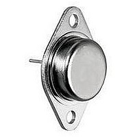
P CH MOSFET, -100V, 18A, TO-204AA
Manufacturer
International Rectifier
Type
Power MOSFETr
Datasheet
1.IRF9140.pdf
(7 pages)
Specifications of IRF9140
Transistor Polarity
P Channel
Continuous Drain Current Id
-18A
Drain Source Voltage Vds
-100V
On Resistance Rds(on)
200mohm
Rds(on) Test Voltage Vgs
-10V
Threshold Voltage Vgs Typ
-4V
Transistor Case Style
TO-3
Rohs Compliant
No
Number Of Elements
1
Polarity
P
Channel Mode
Enhancement
Drain-source On-res
0.23Ohm
Drain-source On-volt
100V
Gate-source Voltage (max)
±20V
Continuous Drain Current
18A
Power Dissipation
125W
Operating Temp Range
-55C to 150C
Operating Temperature Classification
Military
Mounting
Through Hole
Pin Count
2 +Tab
Package Type
TO-204AA
Lead Free Status / RoHS Status
Contains lead / RoHS non-compliant
Lead Free Status / RoHS Status
Contains lead / RoHS non-compliant


Electrical Characteristics
Source-Drain Diode Ratings and Characteristics
Thermal Resistance
Note: Corresponding Spice and Saber models are available on International Rectifier Website.
For footnotes refer to the last page
IRF9140
C iss
BV DSS
∆BV DSS /∆T J
R DS(on)
V GS(th)
g fs
I DSS
I GSS
I GSS
Q g
Q gs
Q gd
t d
t r
t d
t f
L S + L D
C oss
C rss
R thJC
R thJA
I S
I SM
V SD
t rr
Q RR
t on
(on)
(off)
2
Parameter
Continuous Source Current (Body Diode)
Pulse Source Current (Body Diode)
Diode Forward Voltage
Reverse Recovery Time
Reverse Recovery Charge
Forward Turn-On Time
Parameter
Junction-to-Case
Junction-to-Ambient
Parameter
Drain-to-Source Breakdown Voltage
Temperature Coefficient of Breakdown
Voltage
Static Drain-to-Source On-State
Resistance
Gate Threshold Voltage
Forward Transconductance
Zero Gate Voltage Drain Current
Gate-to-Source Leakage Forward
Gate-to-Source Leakage Reverse
Total Gate Charge
Gate-to-Source Charge
Gate-to-Drain (‘Miller’) Charge
Turn-On Delay Time
Rise Time
Turn-Off Delay Time
Fall Time
Total Inductance
Input Capacitance
Output Capacitance
Reverse Transfer Capacitance
@ Tj = 25°C (Unless Otherwise Specified)
Intrinsic turn-on time is negligible. Turn-on speed is substantially controlled by L S + L D .
Min Typ Max Units
—
—
Min Typ Max Units
—
—
—
—
—
-100
Min
-2.0
6.2
3.7
7.0
—
—
—
—
—
—
—
31
—
—
—
—
—
—
—
—
—
—
170
—
—
—
—
-0.087
1400
Typ Max Units
600
200
1.0
6.1
—
—
—
—
—
—
—
—
—
—
—
—
—
—
—
—
30
-5.0
280
-18
-72
3.6
0.23
-250
-100
35.2
-4.0
°C/W
100
0.2
-25
60
13
35
85
85
65
—
—
—
—
—
—
n S
µC
V
A
V/°C
S ( )
nH
nA
ns
µA
nC
pF
Ω
V
V
Soldered to a 2” square copper-clad board
Ω
T j = 25°C, I F = -18A, di/dt ≤ -100A/µs
T
j
= 25°C, I S =-18A, V GS = 0V
Measured from drain lead (6mm/
0.25in. from package) to source lead
(6mm/0.25in. from package)
Reference to 25°C, I D = -1.0mA
V DS > -15V, I DS = -11A
V GS = -10V, I D = -11A
V GS =-10V, I D = -18A
V DS = V GS , I D = -250µA
Test Conditions
Test Conditions
V GS = 0V, I D = -1.0mA
V GS =-10V, R G = 9.1Ω
V DD = -50V, I D = -18A,
V GS =-10V, ID = -18A
V GS = 0V, V DS = -25V
V GS = 0V, T J = 125°C
Test Conditions
V DS = -80V, V GS =0V
V DD ≤ -50V
V DS = -80V
V GS = -20V
f = 1.0MHz
V DS = -50V
V GS = 20V
www.irf.com
Related parts for IRF9140
Image
Part Number
Description
Manufacturer
Datasheet
Request
R

Part Number:
Description:
SCHOTTKY RECTIFIER
Manufacturer:
International Rectifier Corp.
Datasheet:
Part Number:
Description:
SCHOTTKY RECTIFIER
Manufacturer:
International Rectifier Corp.
Datasheet:
Part Number:
Description:
SCHOTTKY RECTIFIER
Manufacturer:
International Rectifier Corp.
Datasheet:
Part Number:
Description:
SCHOTTKY RECTIFIER
Manufacturer:
International Rectifier Corp.
Datasheet:
Part Number:
Description:
SCHOTTKY RECTIFIER
Manufacturer:
International Rectifier Corp.
Datasheet:
Part Number:
Description:
SCHOTTKY RECTIFIER
Manufacturer:
International Rectifier Corp.
Datasheet:
Part Number:
Description:
SCHOTTKY RECTIFIER
Manufacturer:
International Rectifier Corp.
Datasheet:
Part Number:
Description:
SCHOTTKY RECTIFIER
Manufacturer:
International Rectifier Corp.
Datasheet:
Part Number:
Description:
SCHOTTKY RECTIFIER
Manufacturer:
International Rectifier Corp.
Datasheet:
Part Number:
Description:
SCHOTTKY RECTIFIER
Manufacturer:
International Rectifier Corp.
Datasheet:
Part Number:
Description:
SCHOTTKY RECTIFIER
Manufacturer:
International Rectifier Corp.
Datasheet:
Part Number:
Description:
SCHOTTKY RECTIFIER
Manufacturer:
International Rectifier Corp.
Datasheet:
Part Number:
Description:
SCHOTTKY RECTIFIER
Manufacturer:
International Rectifier Corp.
Datasheet:
Part Number:
Description:
SCHOTTKY RECTIFIER
Manufacturer:
International Rectifier Corp.
Datasheet:
Part Number:
Description:
SCHOTTKY RECTIFIER
Manufacturer:
International Rectifier Corp.
Datasheet: