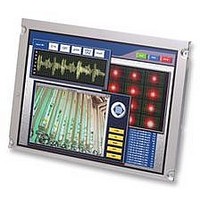
NL3224BC35-20 NEC, NL3224BC35-20 Datasheet - Page 12

NL3224BC35-20
Manufacturer Part Number
NL3224BC35-20
Description
DISPLAY, LCD GRAPHIC, 320 X 240 DOTS
Manufacturer
NEC
Datasheet
1.NL3224BC35-20.pdf
(37 pages)
Specifications of NL3224BC35-20
Viewing Area (h X W)
83.52mm X 111.36mm
Supply Voltage
5V
Display Mode
Active
Rohs Compliant
Yes
Lcd Display Type
TFT
Interface Type
CMOS
Lead Free Status / RoHS Status
Lead free / RoHS Compliant
Available stocks
Company
Part Number
Manufacturer
Quantity
Price
Company:
Part Number:
NL3224BC35-20
Manufacturer:
NEC
Quantity:
1 000
Company:
Part Number:
NL3224BC35-20R
Manufacturer:
TRULY
Quantity:
1 000
4.4 POWER SUPPLY VOLTAGE SEQUENCE
4.4.1 LCD panel signal processing board
4.4.2 Inverter (Option)
Display signals,
Function signals
Note1: In terms of voltage variation (voltage drop) while VCC rising edge is below 3.0V in "VCC=
Note2: Display signals (CLK, Hsync, Vsync, DE, DATA (R0 to R5, G0 to G5, B0 to B5)) and
Note1: These are the display and function signals for LCD panel signal processing board.
Note2: The backlight should be turned on within the valid period of display and function signals, in
Note1
VCC
Note2
Display signals,
Function signals
3.3V" or 4.75V in "VCC= 5.0V", a protection circuit may work, and then this product may not
work.
function signals (DPSH, DPSV, Q/V) must be Low or High-impedance, exclude the VALID
period (See above sequence diagram), in order to avoid that internal circuits is damaged.
If some of display and function signals of this product are cut while this product is working,
even if the signal input to it once again, it might not work normally. VCC should be cut when
the display and function signals are stopped.
order to avoid unstable data display.
VDDB
Note1
3.0V or 4.75V
0V
0ms < t < 35ms
DATA SHEET DOD-PP-0297 (15th edition)
ON
Tr < 20ms
VALID period
Note2
VALID period
OFF
0ms < t < 35ms
NL3224BC35-20
Toff >200ms
ON
12


