CNY17G-3 Vishay, CNY17G-3 Datasheet
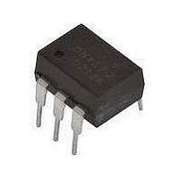
Optocoupler

CNY17G-3

Manufacturer Part Number
CNY17G-3
Description
Optocoupler
Manufacturer
Vishay
Datasheet

Specifications of CNY17G-3

Leaded Process Compatible
Yes
Forward Current
60 mA
Maximum Input Diode Current
60 mA
Maximum Reverse Diode Voltage
5 V
Output Device
Transistor With Base
Output Type
DC
Configuration
1
Input Type
DC
Maximum Collector Emitter Voltage
32 V
Maximum Collector Emitter Saturation Voltage
300 mV
Isolation Voltage
3750 Vrms
Current Transfer Ratio
200 %
Maximum Forward Diode Voltage
1.6 V
Maximum Collector Current
50 mA
Maximum Power Dissipation
250 mW
Maximum Operating Temperature
+ 100 C
Minimum Operating Temperature
- 55 C
Package / Case
PDIP-6
Lead Free Status / RoHS Status
Lead free / RoHS Compliant
Lead Free Status / RoHS Status
Lead free / RoHS Compliant, Lead free / RoHS Compliant

Available stocks

Company
Part Number
Manufacturer
Quantity
Price
Part Number:
CNY17G-3
Quantity:
172
Part Number:
CNY17G-3
Quantity:
5 510
Part Number:
CNY17G-3
Manufacturer:
MAXIM
Quantity:
5 510
Part Number:
CNY17G-3
Manufacturer:
VISHAY/威世
Quantity:
20 000
Part Number:
CNY17G-3SD
Manufacturer:
FAIRCHILD/仙童
Quantity:
20 000
DESCRIPTION
The CNY17G consists of a phototransistor optically coupled
to a gallium arsenide infrared-emitting diode in a 6 pin plastic
dual inline package.
AGENCY APPROVALS
• UL1577, file no. E52744, double protection
• BSI: BS EN 60065, BS EN 60950-1
• DIN EN 60747-5-5 (VDE 0884)
• FIMKO (SETI): EN 60950, certificate no. FI25155
Note
G = leadform 10.16 mm; G is not marked on the body.
Document Number: 83886
Rev. 1.6, 13-Oct-09
ORDER INFORMATION
PART
CNY17G-1
CNY17G-2
CNY17G-3
CNY17G-4
Optocoupler, Phototransistor Output, with Base Connection
17201_5
For technical questions, contact:
18537_3
A (+)
B
6
1
C (-)
C
5
2
D E
V
NC
4
3
E
optocoupleranswers@vishay.com
FEATURES
• Isolation materials according to UL94V-O
• Pollution degree 2 (DIN/VDE 0110 part 1 resp.
• Climatic classification 55/110/21 (IEC 60068
• Special construction: therefore, extra low
• Low temperature coefficient of CTR
• Rated
• Isolation test voltage (partial discharge test voltage)
• Rated isolation voltage V
• Thickness through insulation = 0.4 mm
• Creepage current resistance according to
• CTR offered in 4 groups
• Compliant to RoHS directive 2002/95/EC and in
APPLICATIONS
• Switch-mode power supplies
• Line receiver
• Computer peripheral interface
• Microprocessor system interface
• Circuits for safe protective separation against electrical
IEC 60664)
part 1)
coupling capacity of typical 0.3 pF, high common
mode rejection
V
V
IEC 60112 comparative tracking index: CTI = 275
accordance to WEEE 2002/96/EC
shock according to safety class II (reinforced isolation):
- for appl. class I - IV at mains voltage ≤ 300 V
- for appl. class I - III at mains voltage ≤ 600 V
according to DIN EN 60747-5-5 (VDE 0884)
IOTM
pd
= 1.6 kV
= 6 kV peak
impulse
CTR 100 % to 200 %, DIP-6
CTR 160 % to 320 %, DIP-6
CTR 63 % to 125 %, DIP-6
CTR 40 % to 80 %, DIP-6
Vishay Semiconductors
REMARKS
voltage
IORM
= 850 V
(transient
RMS
CNY17G
www.vishay.com
overvoltage)
VDE 0303/
1

Related parts for CNY17G-3

CNY17G-3 Summary of contents

Page 1

... UL1577, file no. E52744, double protection • BSI 60065 60950-1 • DIN EN 60747-5-5 (VDE 0884) • FIMKO (SETI): EN 60950, certificate no. FI25155 ORDER INFORMATION PART CNY17G-1 CNY17G-2 CNY17G-3 CNY17G-4 Note G = leadform 10.16 mm not marked on the body. Document Number: 83886 For technical questions, contact: Rev. 1.6, 13-Oct-09 FEATURES ...

Page 2

... CNY17G Vishay Semiconductors ABSOLUTE MAXIMUM RATINGS PARAMETER INPUT Reverse voltage Forward current Forward surge current Power dissipation Junction temperature OUTPUT Collector emitter voltage Emitter collector voltage Collector current Collector peak current Power dissipation Junction temperature COUPLER Isolation test voltage (RMS) Total power dissipation ...

Page 3

... Fig Derating Diagram Document Number: 83886 For technical questions, contact: Rev. 1.6, 13-Oct-09 Optocoupler, Phototransistor Output, with Base Connection PART CNY17G-1 CNY17G CNY17G-3 CNY17G-4 CNY17G-1 CNY17G CNY17G-3 CNY17G-2 TEST CONDITION SYMBOL diss V IOTM T si TEST CONDITION SYMBOL Hz ISO CTI 100 %, test ...

Page 4

... CNY17G Vishay Semiconductors SWITCHING CHARACTERISTICS PARAMETER Delay time Rise time Fall time Storage time Turn-on time Turn-off time Turn-on time Turn-off time + mA; adjusted through 0. µs p Channel I Channel II 50 100 95 10900 Fig Test Circuit, Non-Saturated Operation + Ω 0. µs p Channel I Channel II 50 Ω ...

Page 5

... Fig Relative Current Transfer Ratio vs. Ambient Temperature Document Number: 83886 For technical questions, contact: Rev. 1.6, 13-Oct-09 Optocoupler, Phototransistor Output, with Base Connection 80 120 95 11026 Fig Collector Dark Current vs. Ambient Temperature 2.0 1.6 Fig Collector Base Current vs. Forward Current optocoupleranswers@vishay.com CNY17G Vishay Semiconductors 10 000 1000 100 ...

Page 6

... CNY17G Vishay Semiconductors 100 0.1 0 Collector Emitter Voltage (V) 95 11054 CE Fig Collector Current vs. Collector Emitter Voltage 1.0 0.8 0.6 CTR = 50 % used 0.4 0 used Collector Current (mA) 95 11055 C Fig Collector Emitter Saturation Voltage vs. Collector Current 1000 800 600 400 200 0 0.01 0.1 ...

Page 7

... PACKAGE MARKING Document Number: 83886 For technical questions, contact: Rev. 1.6, 13-Oct-09 Optocoupler, Phototransistor Output, with Base Connection 7.12 ± 0.3 4.5 ± 0.3 0.25 1.2 ± 0 CNY17-2 V YWW 24 21764-27 optocoupleranswers@vishay.com CNY17G Vishay Semiconductors 7.62 typ. 6.5 ± 0.3 10.16 (typ.) www.vishay.com 7 ...

Page 8

... Vishay disclaims any and all liability arising out of the use or application of any product described herein or of any information provided herein to the maximum extent permitted by law. The product specifications do not expand or otherwise modify Vishay’ ...

Related keywords