AD9913/PCBZ Analog Devices Inc, AD9913/PCBZ Datasheet - Page 28
AD9913/PCBZ
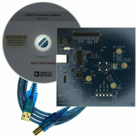
Manufacturer Part Number
AD9913/PCBZ
Description
Eval Board
Manufacturer
Analog Devices Inc
Series
AgileRF™r
Datasheet
1.AD9913BCPZ.pdf
(32 pages)
Specifications of AD9913/PCBZ
Silicon Manufacturer
Analog Devices
Application Sub Type
Direct Digital Synthesizer
Kit Application Type
Clock & Timing
Silicon Core Number
AD9913
Kit Contents
Board
Tool / Board Applications
D/A Converter
Main Purpose
Timing, Direct Digital Synthesis (DDS)
Embedded
No
Utilized Ic / Part
AD9913
Primary Attributes
10-Bit DAC, 32-Bit Tuning Word Width
Secondary Attributes
250MHz, Graphical User Interface
Lead Free Status / RoHS Status
Lead free / RoHS Compliant


AD9913
REGISTER BIT DESCRIPTIONS
The serial I/O port registers span an address range of 0 to 16
(0x00 to 0x10 in hexadecimal notation). This represents a total
of 17 registers. However, one of these registers (0x05) is unused,
yielding a total of 16 available registers.
The registers are not of uniform depth; each contains the
number of bytes necessary for its particular function.
Additionally, the registers are assigned names according to their
functionality. In some cases, a register is given a mnemonic
descriptor. For example, the register at Serial Address 0x00 is
named Control Function Register 1 and is assigned the
mnemonic CFR1.
The following section provides a detailed description of each bit
in the AD9913 register map. For cases in which a group of bits
serve a specific function, the entire group is considered as a
binary word and described in aggregate.
Control Function Register 1 (CFR1)
Address 0x00; 4 bytes are assigned to this register.
Table 10. Bit Description for CFR1
Bit(s)
31:29
28
27
26
25:24
23
22:20
19
18:17
16
15
14
Modulus Enable
Use Internal Profile
Match Pipeline Delays Active
Internal Profile Control
Sync Clock Disable
Clear Auxiliary Accumulator
Clear Phase Accumulator
Bit Name
Open
Open
LSB First
Open
Direct Switch Mode Active
Description
Leave these bits at their default values.
This bit is ignored if linear sweep is disabled.
0 = the auxiliary accumulator is used for linear sweep generation.
1 = the auxiliary accumulator is used for programmable modulus.
0 = profiles are controlled by profile pins; only valid in serial mode.
1 = profiles are controlled by CFR1 [22:20].
0 = the latency across the auxiliary accumulator, the phase offset word, and phase
accumulator are matched.
1 = the latency across the auxiliary accumulator, the phase offset word, and phase
accumulator are not matched.
Leave these bits at the default values.
0 = MSB first format is used.
1 = LSB first format is used.
Ineffective unless Bit 27 = 1. Default is 000
details on how to program these registers during linear sweep, and refer to the Direct
Switch Mode section for details on how to program these registers in direct switch mode.
0 = the SYNC_CLK pin is active.
1 = the SYNC_CLK pin assumes a static Logic 0 state (disabled). In this state, the pin drive
logic is shut down, minimizing the noise generated by the digital circuitry.
Leave these bits in their default values.
0 = direct switch mode is disabled.
1 = direct switch mode is enabled.
0 = normal operation of the auxiliary accumulator (default).
1 = asynchronous, static reset of the auxiliary accumulator. The ramp accumulator remains
reset as long as this bit remains set. This bit is synchronized with either an I/O update or a
profile change and the next rising edge of SYNC_CLK.
0 = normal operation of the DDS phase accumulator (default).
1 = asynchronous, static reset of the DDS phase accumulator.
Rev. A | Page 28 of 32
This section is organized in sequential order of the serial
addresses of the registers. Each subheading includes the register
name and optional register mnemonic (in parentheses). Also
given is the serial address in hexadecimal format and the
number of bytes assigned to the register.
Following each subheading is a table containing the individual
bit descriptions for that particular register. The location of the
bit(s) in the register are indicated by a single number or a pair
of numbers separated by a colon. A pair of numbers (A:B)
indicates a range of bits from the most significant (A) to the
least significant (B). For example, 5:2 implies Bit Position 5
down to Bit Position 2, inclusive, with Bit 0 identifying the LSB
of the register.
Unless otherwise stated, programmed bits are not trans-
ferred to their internal destinations until the assertion of
the I/O_UPDATE pin.
2
. Refer to the Linear Sweep Mode section for
Related parts for AD9913/PCBZ
Image
Part Number
Description
Manufacturer
Datasheet
Request
R


Part Number:
Description:
±1.7g Dual-Axis IMEMS Accelerometer Evaluation Board
Manufacturer:
Analog Devices Inc
Datasheet:

Part Number:
Description:
Inertial Sensor Evaluation System
Manufacturer:
Analog Devices Inc
Datasheet:
Part Number:
Description:
Manufacturer:
Analog Devices Inc
Datasheet:
Part Number:
Description:
Manufacturer:
Analog Devices Inc
Datasheet:
Part Number:
Description:
Manufacturer:
Analog Devices Inc
Datasheet:
Part Number:
Description:
Manufacturer:
Analog Devices Inc
Datasheet:
Part Number:
Description:
Manufacturer:
Analog Devices Inc
Datasheet:
Part Number:
Description:
Manufacturer:
Analog Devices Inc
Datasheet:
Part Number:
Description:
Manufacturer:
Analog Devices Inc
Datasheet:
Part Number:
Description:
Manufacturer:
Analog Devices Inc
Datasheet:
Part Number:
Description:
Manufacturer:
Analog Devices Inc
Datasheet:
Part Number:
Description:
Manufacturer:
Analog Devices Inc
Datasheet: