LS013B4DN01 Sharp Microelectronics, LS013B4DN01 Datasheet - Page 15
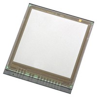
LS013B4DN01
Manufacturer Part Number
LS013B4DN01
Description
LCD Graphic Display Modules & Accessories 1.35 96x96 w/o FPC Mono Memory LCD
Manufacturer
Sharp Microelectronics
Datasheet
1.LS013B4DN01.pdf
(29 pages)
Specifications of LS013B4DN01
Pixel Density
96 x 96
Module Size (w X H X T)
28.2 mm x 32.34 mm x 1.4 mm
Viewing Area (w X H)
24.192 mm x 24.192 mm
Operating Temperature Range
- 20 C to + 70 C
Attached Touch Screen
No
Display Mode
Color - TFT
Product
TFT-LCD Module
Lead Free Status / RoHS Status
Lead free / RoHS Compliant


6-5-2 Data Renew Mode
SCS
SI
SCLK
GL(n-1)th Line
D95
tsSCS
Updates multiple line data. (M0=”H”, M2=”L”)
tsSI
※Refer to 6-6) Input Signal and Display for gate line address setting.
※Input data continuously.
※M1: Frame inversion flag is enabled when EXTMODE=”L”.
※When SCS becomes L, M0 and M2 are cleared.
※In renew mode (When M2=”H”) do “All Clear”, and set P1 through P96 as L.
D96
※In terms of Data writing period
Data has been stored in 1st latch block of Binary driver on Panel.
※In term of Data transfer period
As an example, the 1st latch block in binary driver which stored the data of 1st gate line"GL1"output the data to GL1 and store the data
for 2nd gateline"GL2" at same time.
・M0:Mode flag: If M0 is "H" then Data refresh mode "Pixel data will be updated, If M0 is "L" then display mode "Pixel data is held"
・M1:LC polarity inversion flag: If M1is "H" then VCOM="H" is output. If M1 is "L" then VCOM="L" is output.
・M2:All flags are cleared. If M2 is L then all flags are cleared.
・D1 - D96:Display data: If D* is "L" then Black display can be appeared, if D* is "H" then White display can be appeared
・DUMMY DATA: Dummy data. Don't care but "L" is recommended
M0
DUMMY DATA(don't care)
In addition, if EXTMODE is set as "H", M1 set value doesn't matter.
When all clear are needed, refer to "all clear timing chart"
thSI
M1
(8ck(Dymmy)+7ck(address)+1ck(Dummy)=16ck)
M2
Mode selection period
(3ck+5ckDMY)
DMY
AG0
Data transfer period
DMY
AG1
twSCLKL
DMY
DMY
AG4
twSCLKH
GL(n)th line
DMY
AG5
AG0
AG6
AG1
DMY
twSCSH
twSCSH
Gate line address period
(7ck+1ckDMY)
AG2
D1
AG3
D2
GL1
AG4
Data writing period
SPEC No.
(96ck)
AG5
LCY-12T09302A
D94
AG6
D95
DMY
D96
D1
D2
D3
Data transfer period
D4
Data transfer period
(96ck)
DUMMY DAT A(don't care)
(16ck)
MODEL No.
D93
D94
LS013B4DN01
D95
D96
DUMMY DATA(don't care)
(8ck(Dummy)+7ck(address)+1ck(Dummy)=16ck)
Data transfer period
AG0
thSCS
AG1
GL2
PAGE
AG5
twSCSL
AG6
DMY
13
D1
D2
Related parts for LS013B4DN01
Image
Part Number
Description
Manufacturer
Datasheet
Request
R

Part Number:
Description:
IC FLASH 32MBIT 110NS 56SSOP
Manufacturer:
Sharp Microelectronics
Datasheet:

Part Number:
Description:
IC FLASH 16MBIT 100NS 56TSOP
Manufacturer:
Sharp Microelectronics
Datasheet:

Part Number:
Description:
IC FLASH 64MBIT 120NS 56TSOP
Manufacturer:
Sharp Microelectronics
Datasheet:

Part Number:
Description:
IC FLASH 16MBIT 90NS 48TSOP
Manufacturer:
Sharp Microelectronics
Datasheet:
Part Number:
Description:
IC SRAM 16KBIT 100NS 24DIP
Manufacturer:
Sharp Microelectronics
Datasheet:
Part Number:
Description:
IC SRAM 16KBIT 100NS 24SOP
Manufacturer:
Sharp Microelectronics
Datasheet:
Part Number:
Description:
IC SRAM 64KBIT 100NS 28DIP
Manufacturer:
Sharp Microelectronics
Datasheet:
Part Number:
Description:
IC SRAM 64KBIT 100NS 28SOP
Manufacturer:
Sharp Microelectronics
Datasheet:
Part Number:
Description:
IC SRAM 64KBIT 100NS 28SOP
Manufacturer:
Sharp Microelectronics
Datasheet:
Part Number:
Description:
IC SRAM 256KBIT 70NS 28DIP
Manufacturer:
Sharp Microelectronics
Datasheet:
Part Number:
Description:
IC FLASH 8MBIT 90NS 48TSOP
Manufacturer:
Sharp Microelectronics
Datasheet:
Part Number:
Description:
IC FLASH 8MBIT 85NS 40TSOP
Manufacturer:
Sharp Microelectronics
Datasheet:
Part Number:
Description:
IC FLASH 8MBIT 85NS 40TSOP
Manufacturer:
Sharp Microelectronics
Datasheet:
Part Number:
Description:
IC FLASH 16MBIT 90NS 48TSOP
Manufacturer:
Sharp Microelectronics
Datasheet:
Part Number:
Description:
IC FLASH 16MBIT 70NS 56TSOP
Manufacturer:
Sharp Microelectronics
Datasheet: