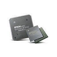
S1D13743B00C400 Epson, S1D13743B00C400 Datasheet - Page 2

S1D13743B00C400
Manufacturer Part Number
S1D13743B00C400
Description
LCD Drivers 464K SRAM Enhanced Dbl buff WQVGA TFT
Manufacturer
Epson
Datasheet
1.S1D13742F01A200.pdf
(2 pages)
Specifications of S1D13743B00C400
Operating Supply Voltage
1.5 V
Package / Case
QFP-144
Attached Touch Screen
No
Lead Free Status / RoHS Status
Lead free / RoHS Compliant
Integrated Frame Buffer
CPU Interface
Panel Support
Miscellaneous
CONTACT YOUR SALES REPRESENTATIVE FOR THESE COMPREHENSIVE DESIGN TOOLS
• S1D13742 Technical
• S1D13742 Evaluation
©SEIKO EPSON CORPORATION 2005 - 2007. All rights reserved.
Information in this document is subject to change without notice. You may download and use this document, but only for your own use in evaluating Seiko Epson/EPSON products. You
may not modify the document. Epson Research and Development, Inc. disclaims any representation that the contents of this document are accurate or current. The Programs/Technologies
described in this document may contain material protected under U.S. and/or International Patent laws.
EPSON is a registered trademark of Seiko Epson Corporation. All other trademarks are the property of their respective owners.
•
•
•
•
•
•
•
•
•
•
•
•
•
•
Documentation
Boards
Hong Kong
Epson Hong Kong Ltd.
20/F., Harbour Centre
25 Harbour Road
Wanchai, Hong Kong
Tel: 2585-4600
Fax: 2827-4346
http://www.epson.com.hk/
Japan
Seiko Epson Corporation
IC International Sales Group
421-8, Hino, Hino-shi
Tokyo 191-8501, Japan
Tel: 042-587-5812
Fax: 042-587-5564
http://www.epson.co.jp/
DESCRIPTION
Embedded 768K byte SRAM display buffer.
8/16-bit Intel 80 interface (used for display or register
data).
Chip select is used to select device. When inactive, any
input data/command will be ignored.
Active Matrix TFT interface.
18/36-bit interface.
Supports resolutions up to 800x480.
Internal programmable PLL.
Single MHz clock input: CLKI.
CLKI available as CLKOUT (separate CLKOUTEN pin
associated with output).
Hardware / Software Power Save mode.
Input pin to Enable/Disable Power Save Mode.
General Purpose Input/Output pins are available
(GPIO[7:0]).
COREVDD 1.5 volts and IOVDD 1.65 ~ 3.6 volts
FCBGA 121-pin or QFP20 144-pin package
2
GRAPHICS
S1D13742
• CPU Independent
• Royalty Free source level
Software Utilities
driver code
Europe
Epson Europe Electronics GmbH
Riesstrasse 15
80992 Munich, Germany
Tel: 089-14005-0
Fax: 089-14005-110
http://www.epson-electronics.de/
North America
Epson Electronics America, Inc.
2580 Orchard Parkway
San Jose, CA 95131, USA
Tel: (408) 922-0200
Fax: (408) 922-0238
http://www.eea.epson.com/
Revision 3.01
Digital Video
Display Features
•
•
•
•
•
•
•
•
•
RGB: 8:8:8, 6:6:6, 5:6:5 (8:8:8 will be truncated to 16 or 18
bpp).
YUV 4:2:2, 4:2:0 (Internal YUV to RGB Converter stored as
16 or 18 bpp).
16/18 bit-per-pixel (bpp) color depths.
16 bpp to 18 bpp Input Data conversion.
All display writes are handled by window apertures/position
for complete or partial display updates. All window coordi-
nates are referenced to top left corner of the displayed image
(even in a rotated display, the top-left corner is maintained
and no host side translation need take place).
SwivelView™: 90°, 180°, 270° counter-clockwise hardware
rotation of display image. All displayed windows can have
independent rotation. No additional programming necessary
when enabling these modes.
Double-Buffer available to prevent image tearing during
streaming input. Resolutions supported must fit inside 384K
bytes (½ of total available display buffer). Typical resolution of
352x416.
Pixel Doubling: Horizontal and Vertical averaging for smooth
doubling of a single window.
Pixel Halving: no limitation on number of windows.
Singapore
Epson Singapore Pte Ltd
1 HarbourFront Place #03-02
HarbourFront Tower One
Singapore, 098633
Tel: (65) 6586-5500
Fax: (65) 6271-3182
http://www.epson.com.sg/
Taiwan
Epson Taiwan Technology & Trading Ltd.
14F, No. 7
Song Ren Road
Taipei 110
Tel: 02-8786-6688
Fax: 02-8786-6677
http://www.epson.com.tw/
X63A-C-001-03


