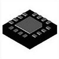
MAX17149ETE+ Maxim Integrated Products, MAX17149ETE+ Datasheet - Page 18

MAX17149ETE+
Manufacturer Part Number
MAX17149ETE+
Description
LED Drivers 6-String WLED Driver
Manufacturer
Maxim Integrated Products
Datasheet
1.MAX17129ETE.pdf
(20 pages)
Specifications of MAX17149ETE+
Operating Supply Voltage
3 V to 26 V
Maximum Supply Current
4 mA
Maximum Power Dissipation
1176 mW
Maximum Operating Temperature
+ 85 C
Mounting Style
SMD/SMT
Package / Case
TQFN-16
Minimum Operating Temperature
- 40 C
Lead Free Status / RoHS Status
Lead free / RoHS Compliant
Low-Cost, 6-String WLED Drivers with
Quick-PWM Step-Up Converter
Careful PCB layout is important for proper operation. Use
the following guidelines for good PCB layout:
1) Minimize the area of high current-switching loop
2) Connect high-current input and output components
3) Create a ground island (PGND) consisting of the
18
of the rectifier diode, internal MOSFET, and output
capacitor to avoid excessive switching noise.
with short and wide connections. The high-current
input loop goes from the positive terminal of the input
capacitor to the inductor, to the internal MOSFET,
then to the input capacitor’s negative terminal. The
high-current output loop is from the positive terminal
of the input capacitor to the inductor, to the rectifier
diode, to the positive terminal of the output capaci-
tors, reconnecting between the output capacitor and
input capacitor ground terminals. Avoid using vias
in the high-current paths. If vias are unavoidable,
use multiple vias in parallel to reduce resistance and
inductance.
input and output capacitor ground. Connect all
PCB Layout Guidelines
4) Place the IN pin and V
5) Minimize the size of the LX node while keeping it wide
Refer to the MAX17129/MAX17149 evaluation kit for an
example of proper board layout.
these together with short, wide traces or a small
ground plane. Maximizing the width of the power
ground traces improves efficiency and reduces out-
put-voltage ripple and noise spikes. Create an analog
ground island (GND) consisting of ISET, IN, V
nections, and the devices’ exposed backside pad.
Connect the GND and PGND islands by connecting
the GND pins directly to the exposed backside pad.
Make no other connections between these separate
ground planes.
close to the device as possible. The ground connec-
tion of the bypass capacitors should be connected
directly to the GND pins with a wide trace.
and short. If possible, avoid running the LX node from
one side of the PCB to the other. Use DC traces as
shield if necessary.
CC
pin bypass capacitors as
CC
con-


