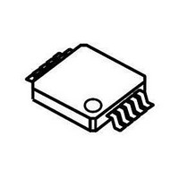
NJU6060V-TE1 NJR, NJU6060V-TE1 Datasheet

NJU6060V-TE1
Specifications of NJU6060V-TE1
Related parts for NJU6060V-TE1
NJU6060V-TE1 Summary of contents
Page 1
... FEATURES # Controls the 3-color LED Separately (ILED=10mA x 3 outputs) # Built-in PWM Luminance Control (32 steps Built-in 8bit serial Interface Circuit # Built-in Oscillation Circuit # Operating Voltage for Step-up Circuits # Package # CMOS Technology Ver.2004-04-16 ! PACKAGE OUTLINE : 2.4V to 5.5V : SSOP-10 NJU6060 NJU6060V - 1 - ...
Page 2
NJU6060 ! PIN CONNECTIONS (TOP VIEW) ! PIN DESCRIPTIONS No. PIN NAME RSTb 3 CSb 4 CLK 5 DATA 6 OSC LED1 9 LED2 10 LED3 - 2 - TYPE Power V ...
Page 3
BLOCK DIAGRAM V DD OSC RSTb C / CSb P F CLK U DATA FUNCTIONAL DESCRIPTIONS (1) Description for each blocks (1-1) PWM Luminance Control The NJU6060 incorporates three channel of 32 steps ...
Page 4
NJU6060 (2) Instructions 3 line type serial interface using a setup of PWM data, ON/OFF of Light Emitting Diode, etc. are made. The input data and latched at rising edge of chip shift clock (CLK) and the 8-bit data are ...
Page 5
PWM Frequency set / OSC ON/OFF / Output port ON/OFF This instruction set the PWM Frequency, Oscillator ON/OFF and Output port ON/OFF. PWM Frequency set / OSC ON/OFF / Output port ON/OFF ...
Page 6
NJU6060 Example ) Set Output PWM waveform of LED1 to LED3 terminal, shown below: - LED1 PWM Phase set D = LED2 PWM Phase set D = LED3 PWM Phase set D =1, D ...
Page 7
Serial Interface The NJU6060 interface with MPU by Serial Interface, control for LED. CSb CLK * D7 SIO Note1) Data is not concerned with the signal of CSb but is read into the internal shift register by the rising ...
Page 8
NJU6060 ! ABSOLUTE MAXIMUMN RATINGS PARAMETERS VDD Power Supply Driver Off Break Down Voltage Driver On Break Down Voltage Input Voltage Power Dissipation Operating Temperature Storage Temperature Note1 all conditions SS Note2) If the LSI was ...
Page 9
DC ELECTRICAL CHARACTERISTICS PARAMETERS SYMBOL V Power Supply DD Input “H” Level Voltage Input “L” Level Voltage Input “H” Level Current Input “L” Level Current Output Off Leak Current Output “L” Level Voltage Oscillation Frequency Reset “L” Level Pulse ...
Page 10
NJU6060 Relation between oscillation frequency and LCD frame frequency Set Output PWM waveform of LED1 to LED3 terminal, shown below: - LED1 PWM Phase set D = LED2 PWM Phase set D = LED3 ...
Page 11
AC ELECTRICAL CHARACTERISTICS PARAMETERS “L” Level CLK Clock Width “H” Level CLK Clock Width Data Set-Up Time Data Hold Time CSb Set-Up Time CSb Hold Time CLK Wait Time Rising Time Falling Time Serial Input Timing CSb CLK DATA ...
Page 12
NJU6060 ! APPLICATION CIRCUIT CPU Resistor Selection Example 10mA, V LED Note) VF and VOL are depended on the situation. And decide the optimum values by the actual test when RLED is selected. - ...


