1N5352BG ON Semiconductor, 1N5352BG Datasheet - Page 2
1N5352BG
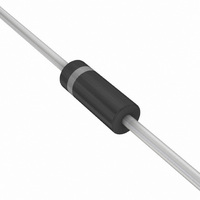
Manufacturer Part Number
1N5352BG
Description
DIODE ZENER 15V 5W AXIAL
Manufacturer
ON Semiconductor
Series
Surmetic™r
Specifications of 1N5352BG
Voltage - Zener (nom) (vz)
15V
Voltage - Forward (vf) (max) @ If
1.2V @ 1A
Current - Reverse Leakage @ Vr
1µA @ 11.5V
Tolerance
±5%
Power - Max
5W
Impedance (max) (zzt)
2.5 Ohm
Mounting Type
Through Hole
Package / Case
Axial
Operating Temperature
-65°C ~ 200°C
Zener Voltage
15 V
Voltage Tolerance
5 %
Zener Current
315 mA
Power Dissipation
5 W
Maximum Reverse Leakage Current
1 uA
Maximum Zener Impedance
2.5 Ohms
Maximum Operating Temperature
+ 200 C
Mounting Style
SMD/SMT
Minimum Operating Temperature
- 65 C
Voltage Regulation Accuracy
250 mV
Current, Forward
1 A
Current, Reverse
75 mA
Current, Surge
6.3 A
Package Type
Case 17
Primary Type
Zener
Temperature, Junction, Maximum
+200 °C
Temperature, Operating
-65 to +200 °C
Voltage, Forward
1.2 V
Voltage, Reverse
15 V
Zener Voltage Vz Typ
15V
Power Dissipation Pd
5W
Operating Temperature Range
-65°C To +200°C
Diode Case Style
017AA
No. Of Pins
2
Diode Type
Zener
Forward Voltage Vf Max
15V
Rohs Compliant
Yes
Lead Free Status / RoHS Status
Lead free / RoHS Compliant
Other names
1N5352BG
1N5352BGOS
1N5352BGOS
Available stocks
Company
Part Number
Manufacturer
Quantity
Price
Company:

Part Number:
1N5352BG
Manufacturer:
ON
Quantity:
9 377
Company:
Part Number:
1N5352BG
Manufacturer:
ON
Quantity:
30 000
Part Number:
1N5352BG
Manufacturer:
ON/安森美
Quantity:
20 000


Devices listed in bold, italic are ON Semiconductor Preferred devices. Preferred devices are recommended choices for future use and best overall value.
1. TOLERANCE AND TYPE NUMBER DESIGNATION: The JEDEC type numbers shown indicate a tolerance of ±5%.
2. ZENER VOLTAGE (V
3. SURGE CURRENT (I
4. VOLTAGE REGULATION (DV
5. MAXIMUM REGULATOR CURRENT (I
†The “G'' suffix indicates Pb-Free package or Pb-Free packages are available.
ELECTRICAL CHARACTERISTICS
otherwise noted, V
ELECTRICAL CHARACTERISTICS
1N5333B, G
1N5337BG
1N5338BG
1N5339B, G
1N5341B, G
1N5342BG
1N5347B, G
1N5334BG
1N5335BG
1N5336BG
1N5340B, G
1N5343BG
1N5344B, G
1N5345B, G
1N5346BG
Symbol
40 ±10 ms prior to reading. Mounting contacts are located 3/8″ to 1/2″ from the inside edge of mounting clips to the body of the diode
(T
PW, of 8.3 ms. The data given in Figure 5 may be used to find the maximum surge current for a square wave of any pulse width between
1 ms and 1000 ms by plotting the applicable points on logarithmic paper. Examples of this, using the 3.3 V and 200 V zener are shown in
Figure 6. Mounting contact located as specified in Note 2 (T
of the I
contact located as specified in Note 2 (T
it applies only to the B-suffix device. The actual I
T
DV
Z
Z
I
Device
I
I
V
(Note 1)
V
V
ZM
ZK
I
I
I
L
ZT
ZK
ZT
R
R
A
F
R
Z
F
= 75°C at 3/8″ maximum from the device body.
Z
= 25°C +8°C, -2°C).
Z
†
max value listed in the electrical characteristics table. The test current time duration for each V
Reverse Zener Voltage @ I
Reverse Current
Maximum Zener Impedance @ I
Reverse Current
Maximum Zener Impedance @ I
Reverse Leakage Current @ V
Breakdown Voltage
Forward Current
Forward Voltage @ I
Maximum Surge Current @ T
Reverse Zener Voltage Change
Maximum DC Zener Current
1N5333B
1N5334B
1N5335B
1N5336B
1N5337B
1N5338B
1N5339B
1N5340B
1N5341B
1N5342B
1N5343B
1N5344B
1N5345B
1N5346B
1N5347B
Marking
F
Device
= 1.2 V Max @ I
R
Z
): Surge current is specified as the maximum allowable peak, non-recurrent square-wave current with a pulse width,
) and IMPEDANCE (I
3.14
3.42
3.71
4.09
4.47
4.85
5.32
5.70
5.89
6.46
7.13
7.79
8.27
8.65
9.50
Min
Parameter
Zener Voltage (Note 2)
Z
F
): The conditions for voltage regulation are as follows: V
V
F
Z
Nom
= 1.0 A for all types)
(Volts)
3.3
3.6
3.9
4.3
4.7
5.1
5.6
6.0
6.2
6.8
7.5
8.2
8.7
9.1
10
ZT
(T
(T
ZM
A
A
A
A
R
= 25°C
= 25°C +8°C, -2°C).
): The maximum current shown is based on the maximum voltage of a 5% type unit, therefore,
ZT
ZK
= 25°C unless
= 25°C unless otherwise noted, V
Max
3.47
3.78
4.10
4.52
4.94
5.36
5.88
6.30
6.51
7.14
7.88
8.61
9.14
9.56
10.5
ZT
ZM
and I
@ I
for any device may not exceed the value of 5 watts divided by the actual V
380
350
320
290
260
240
220
200
200
175
175
150
150
150
125
mA
ZT
ZK
1N5333B Series
): Test conditions for zener voltage and impedance are as follows: I
Z
Zener Impedance (Note 2)
A
ZT
= 25°C +8°C, -2°C).
2.5
1.5
1.5
1.5
W
@ I
3
2
2
2
1
1
1
1
2
2
2
2
ZT
Z
ZK
400
500
500
500
450
400
400
300
200
200
200
200
200
150
125
W
@ I
F
= 1.2 V Max @ I
ZK
V
mA
I
Z
ZK
1
1
1
1
1
1
1
1
1
1
1
1
1
1
1
Z
V
R
measurements are made at 10% and then at 50%
Zener Voltage Regulator
mA Max
300
150
7.5
50
10
10
10
10
10
Leakage
5
1
1
1
1
5
Current
I
R
F
@ V
= 1.0 A for all types)
Z
I
Volts
R
measurement is 40 ±10 ms. Mounting
F
5.2
5.7
6.2
6.6
6.9
7.6
1
1
1
1
1
1
2
3
3
I
I
I
R
ZT
V
(Note 3)
F
18.7
17.6
16.4
15.3
14.4
13.4
12.7
12.4
10.7
11.5
9.5
9.2
8.6
20
10
I
A
R
(Note 4)
Volts
0.85
0.54
0.49
0.44
0.39
0.25
0.19
0.15
0.15
0.22
0.22
DV
0.8
0.1
0.2
0.2
Z
Z
of the device.
Z
is applied
V
(Note 5)
1440
1320
1220
1100
1010
930
865
790
765
700
630
580
545
520
475
mA
I
ZM
Related parts for 1N5352BG
Image
Part Number
Description
Manufacturer
Datasheet
Request
R

Part Number:
Description:
ON Semiconductor [VOLTAGE REGULATOR]
Manufacturer:
ON Semiconductor
Datasheet:
Part Number:
Description:
357-036-542-201 CARDEDGE 36POS DL .156 BLK LOPRO
Manufacturer:
ON Semiconductor
Datasheet:
Part Number:
Description:
357-036-542-201 CARDEDGE 36POS DL .156 BLK LOPRO
Manufacturer:
ON Semiconductor
Datasheet:
Part Number:
Description:
357-036-542-201 CARDEDGE 36POS DL .156 BLK LOPRO
Manufacturer:
ON Semiconductor
Datasheet:
Part Number:
Description:
357-036-542-201 CARDEDGE 36POS DL .156 BLK LOPRO
Manufacturer:
ON Semiconductor
Datasheet:
Part Number:
Description:
357-036-542-201 CARDEDGE 36POS DL .156 BLK LOPRO
Manufacturer:
ON Semiconductor
Datasheet:
Part Number:
Description:
357-036-542-201 CARDEDGE 36POS DL .156 BLK LOPRO
Manufacturer:
ON Semiconductor
Datasheet:
Part Number:
Description:
357-036-542-201 CARDEDGE 36POS DL .156 BLK LOPRO
Manufacturer:
ON Semiconductor
Datasheet:
Part Number:
Description:
357-036-542-201 CARDEDGE 36POS DL .156 BLK LOPRO
Manufacturer:
ON Semiconductor
Datasheet:
Part Number:
Description:
357-036-542-201 CARDEDGE 36POS DL .156 BLK LOPRO
Manufacturer:
ON Semiconductor
Datasheet:
Part Number:
Description:
357-036-542-201 CARDEDGE 36POS DL .156 BLK LOPRO
Manufacturer:
ON Semiconductor
Datasheet:
Part Number:
Description:
Manufacturer:
ON Semiconductor
Datasheet:
Part Number:
Description:
Manufacturer:
ON Semiconductor
Datasheet:
Part Number:
Description:
Manufacturer:
ON Semiconductor
Datasheet: