1N5352BG ON Semiconductor, 1N5352BG Datasheet - Page 3
1N5352BG
Manufacturer Part Number
1N5352BG
Description
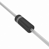
DIODE ZENER 15V 5W AXIAL
Manufacturer
ON Semiconductor
Series
Surmetic™r
Specifications of 1N5352BG
Voltage - Zener (nom) (vz)
15V
Voltage - Forward (vf) (max) @ If
1.2V @ 1A
Current - Reverse Leakage @ Vr
1µA @ 11.5V
Tolerance
±5%
Power - Max
5W
Impedance (max) (zzt)
2.5 Ohm
Mounting Type
Through Hole
Package / Case
Axial
Operating Temperature
-65°C ~ 200°C
Zener Voltage
15 V
Voltage Tolerance
5 %
Zener Current
315 mA
Power Dissipation
5 W
Maximum Reverse Leakage Current
1 uA
Maximum Zener Impedance
2.5 Ohms
Maximum Operating Temperature
+ 200 C
Mounting Style
SMD/SMT
Minimum Operating Temperature
- 65 C
Voltage Regulation Accuracy
250 mV
Current, Forward
1 A
Current, Reverse
75 mA
Current, Surge
6.3 A
Package Type
Case 17
Primary Type
Zener
Temperature, Junction, Maximum
+200 °C
Temperature, Operating
-65 to +200 °C
Voltage, Forward
1.2 V
Voltage, Reverse
15 V
Zener Voltage Vz Typ
15V
Power Dissipation Pd
5W
Operating Temperature Range
-65°C To +200°C
Diode Case Style
017AA
No. Of Pins
2
Diode Type
Zener
Forward Voltage Vf Max
15V
Rohs Compliant
Yes
Lead Free Status / RoHS Status
Lead free / RoHS Compliant
Other names
1N5352BG
1N5352BGOS
1N5352BGOS
Available stocks
Company
Part Number
Manufacturer
Quantity
Price
Company:

Part Number:
1N5352BG
Manufacturer:
ON
Quantity:
9 377
Company:
Part Number:
1N5352BG
Manufacturer:
ON
Quantity:
30 000
Part Number:
1N5352BG
Manufacturer:
ON/安森美
Quantity:
20 000


Devices listed in bold, italic are ON Semiconductor Preferred devices. Preferred devices are recommended choices for future use and best overall value.
6. TOLERANCE AND TYPE NUMBER DESIGNATION: The JEDEC type numbers shown indicate a tolerance of ±5%.
7. ZENER VOLTAGE (V
8. SURGE CURRENT (I
9. VOLTAGE REGULATION (DV
10. MAXIMUM REGULATOR CURRENT (I
†The “G'' suffix indicates Pb-Free package or Pb-Free packages are available.
ELECTRICAL CHARACTERISTICS
1N5349B, G
1N5350B, G
1N5352B, G
1N5353B, G
1N5358B, G
1N5359B, G
1N5361B, G
1N5365B, G
1N5368BG
1N5383B, G
1N5348BG
1N5351BG
1N5354B, G
1N5355B, G
1N5356BG
1N5357BG
1N5360BG
1N5362BG
1N5363BG
1N5364BG
1N5366B, G
1N5367BG
1N5369B, G
1N5370B, G
1N5371BG
1N5372BG
1N5373B, G
1N5374BG
1N5375BG
1N5377BG
1N5378B, G
1N5380BG
1N5381BG
1N5384BG
1N5386BG
1N5387BG
1N5388B, G
40 ±10 ms prior to reading. Mounting contacts are located 3/8″ to 1/2″ from the inside edge of mounting clips to the body of the diode
(T
PW, of 8.3 ms. The data given in Figure 5 may be used to find the maximum surge current for a square wave of any pulse width between
1 ms and 1000 ms by plotting the applicable points on logarithmic paper. Examples of this, using the 3.3 V and 200 V zener are shown in
Figure 6. Mounting contact located as specified in Note 7 (T
of the I
contact located as specified in Note 7 (T
it applies only to the B-suffix device. The actual I
T
Device
(Note 6)
L
A
= 75°C at 3/8″ maximum from the device body.
= 25°C +8°C, -2°C).
Z
†
max value listed in the electrical characteristics table. The test current time duration for each V
1N5348B
1N5349B
1N5350B
1N5351B
1N5352B
1N5353B
1N5354B
1N5355B
1N5356B
1N5357B
1N5358B
1N5359B
1N5360B
1N5361B
1N5362B
1N5363B
1N5364B
1N5365B
1N5366B
1N5367B
1N5368B
1N5369B
1N5370B
1N5371B
1N5372B
1N5373B
1N5374B
1N5375B
1N5377B
1N5378B
1N5380B
1N5381B
1N5383B
1N5384B
1N5386B
1N5387B
1N5388B
Marking
Device
R
Z
): Surge current is specified as the maximum allowable peak, non-recurrent square-wave current with a pulse width,
) and IMPEDANCE (I
10.45
12.35
14.25
16.15
18.05
23.75
25.65
31.35
37.05
40.85
44.65
48.45
71.25
86.45
123.5
142.5
180.5
13.3
15.2
17.1
20.9
22.8
26.6
28.5
34.2
53.2
58.9
64.6
77.9
11.4
Min
152
171
190
114
19
57
95
Zener Voltage (Note 7)
Z
): The conditions for voltage regulation are as follows: V
V
Z
Nom
100
120
130
150
160
180
190
200
(Volts)
11
12
13
14
15
16
17
18
19
20
22
24
25
27
28
30
33
36
39
43
47
51
56
60
62
68
75
82
91
(T
ZM
A
A
= 25°C +8°C, -2°C).
): The maximum current shown is based on the maximum voltage of a 5% type unit, therefore,
13.65
15.75
17.85
19.95
26.25
28.35
34.65
40.95
45.15
49.35
53.55
78.75
95.55
136.5
157.5
199.5
11.55
= 25°C unless otherwise noted, V
Max
12.6
14.7
16.8
18.9
23.1
25.2
29.4
31.5
37.8
58.8
65.1
71.4
86.1
105
126
168
189
210
21
63
ZT
ZM
and I
for any device may not exceed the value of 5 watts divided by the actual V
@ I
125
100
100
100
mA
75
75
70
65
65
65
50
50
50
50
50
40
40
30
30
30
25
25
20
20
20
20
20
15
15
12
10
10
8
8
5
5
5
ZK
ZT
1N5333B Series
): Test conditions for zener voltage and impedance are as follows: I
Z
Zener Impedance (Note 7)
A
ZT
= 25°C +8°C, -2°C).
170
190
330
350
430
450
480
2.5
2.5
2.5
2.5
2.5
2.5
2.5
2.5
3.5
3.5
10
11
14
20
25
27
35
40
42
44
45
65
75
90
W
@ I
3
3
4
5
6
8
3
ZT
Z
ZK
1250
1500
1650
1750
1850
1850
1150
125
125
100
100
120
130
140
150
160
170
190
210
230
280
350
400
500
620
720
760
800
110
75
75
75
75
75
75
75
75
W
@ I
F
= 1.2 V Max @ I
ZK
mA
I
ZK
1
1
1
1
1
1
1
1
1
1
1
1
1
1
1
1
1
1
1
1
1
1
1
1
1
1
1
1
1
1
1
1
1
1
1
1
1
Z
measurements are made at 10% and then at 50%
mA Max
0.5
0.5
0.5
0.5
0.5
0.5
0.5
0.5
0.5
0.5
0.5
0.5
0.5
0.5
0.5
0.5
0.5
0.5
0.5
0.5
0.5
0.5
0.5
0.5
0.5
0.5
0.5
0.5
0.5
0.5
0.5
Leakage
5
2
1
1
1
1
Current
I
R
F
@ V
= 1.0 A for all types)
Z
measurement is 40 ±10 ms. Mounting
Volts
R
10.6
12.2
12.9
13.7
14.4
15.2
16.7
18.2
20.6
21.2
22.8
25.1
27.4
29.7
32.7
35.8
38.8
42.6
45.5
47.1
51.7
62.2
69.2
91.2
98.8
11.5
114
122
137
144
152
8.4
9.1
9.9
19
56
76
(Note 8)
8.0
7.5
7.0
6.7
6.3
6.0
5.8
5.5
5.3
5.1
4.7
4.4
4.3
4.1
3.9
3.7
3.5
3.5
3.1
2.8
2.7
2.5
2.3
2.2
2.1
2.0
1.9
1.8
1.6
1.5
1.3
1.2
1.1
1.1
1.0
0.9
0.9
I
A
R
(Note 9)
Volts
0.25
0.25
0.25
0.25
0.25
0.35
0.45
0.55
0.55
0.65
0.65
1.35
1.52
DV
0.3
0.4
0.4
0.4
0.6
0.6
0.6
0.6
0.7
0.8
0.9
1.0
1.2
1.6
1.8
2.2
2.5
2.5
2.5
3.0
3.0
4.0
5.0
5.0
Z
of the device.
Z
Z
is applied
(Note 10)
52.5
47.5
39.5
36.6
31.6
29.4
26.4
23.6
mA
430
395
365
340
315
295
280
264
250
237
216
198
190
176
170
158
144
132
122
110
100
I
93
86
79
76
70
63
58
25
ZM
Related parts for 1N5352BG
Image
Part Number
Description
Manufacturer
Datasheet
Request
R

Part Number:
Description:
ON Semiconductor [VOLTAGE REGULATOR]
Manufacturer:
ON Semiconductor
Datasheet:
Part Number:
Description:
357-036-542-201 CARDEDGE 36POS DL .156 BLK LOPRO
Manufacturer:
ON Semiconductor
Datasheet:
Part Number:
Description:
357-036-542-201 CARDEDGE 36POS DL .156 BLK LOPRO
Manufacturer:
ON Semiconductor
Datasheet:
Part Number:
Description:
357-036-542-201 CARDEDGE 36POS DL .156 BLK LOPRO
Manufacturer:
ON Semiconductor
Datasheet:
Part Number:
Description:
357-036-542-201 CARDEDGE 36POS DL .156 BLK LOPRO
Manufacturer:
ON Semiconductor
Datasheet:
Part Number:
Description:
357-036-542-201 CARDEDGE 36POS DL .156 BLK LOPRO
Manufacturer:
ON Semiconductor
Datasheet:
Part Number:
Description:
357-036-542-201 CARDEDGE 36POS DL .156 BLK LOPRO
Manufacturer:
ON Semiconductor
Datasheet:
Part Number:
Description:
357-036-542-201 CARDEDGE 36POS DL .156 BLK LOPRO
Manufacturer:
ON Semiconductor
Datasheet:
Part Number:
Description:
357-036-542-201 CARDEDGE 36POS DL .156 BLK LOPRO
Manufacturer:
ON Semiconductor
Datasheet:
Part Number:
Description:
357-036-542-201 CARDEDGE 36POS DL .156 BLK LOPRO
Manufacturer:
ON Semiconductor
Datasheet:
Part Number:
Description:
357-036-542-201 CARDEDGE 36POS DL .156 BLK LOPRO
Manufacturer:
ON Semiconductor
Datasheet:
Part Number:
Description:
Manufacturer:
ON Semiconductor
Datasheet:
Part Number:
Description:
Manufacturer:
ON Semiconductor
Datasheet:
Part Number:
Description:
Manufacturer:
ON Semiconductor
Datasheet: